Friday, September 26, 2014

Simple Guitar Fuzz Circuit

Guitar Fuzz Circuit:
  The input signal is amplified by the two transistors. The distorted output is then clipped by the two diodes and the high frequency noise is filtered from the circuit via the 500pF capacitor.
The 1 M not adjusts the intensity of the fuzz, but this tends to make the unit oscillate. so a 33k resistor is put between the input and ground to stop this. When the pot is at minimum intensity the unit may be switched off to allow normal playing. 


Read more

Active Tone Control Circuit Using a Single Opamp

The input signal is applied to the non-inverting input of the lC which is a Siemens TAA861 operational amplifier.
Bass and treble boost and cut are con_trolled by the potentiometers RV1 and RV2 respectively. Control range is 20 dB of boost or cut at 50 Hz and 15 dB boost or 20 dB of cut at 12 kHz. The overall gain of the circuit at 1 kHz is 15dB and the input impedance is greater than 80 k ohm. Total harmonic distortion for 2.4 volts output is less than 0.5% and remains below 4% for up to 3.5 volts output. Correct law for the potentiometer is antilog. This may be obtained by using slide potentiometers which are mounted in reverse (end-for~end) to normal. Note that equalization is not incorporated in this preamplifier.


This simple single-transistor circuit will give approximately 15 dB boost or cut at 100 Hz and 15 kHz respectively. A low noise audio type transistor is used, and the output can be fed directly into any existing amplifier volume control to which the tone control is to be fitted. A The gain of the circuit is near unity when controls are set in the "flat" position. 


Read more

Thursday, September 25, 2014

How to Generate Electricity from Heat or Body Warmth

The present design exploits the above property of tunnel diodes by having a series connected set of these devices charge a battery with the aid of solar energy


The operating principle of this unique design is remarkably simple. 

 As seen in Fig seven or more Gallium-Indium Antimonide (GISp) tunnel diodes are series connected and titted on a large heatsink, which does not serve to dissipate their power (tunnel diodes get colder as Ur rises), but to effectively accumulate solar, or otherwise applied, heat, whose energy is converted into a charge current for the NiCd battery

When the load is itself a voltage source with fairly low internal  resistance, the negative resistance must, of course, output a f higher voltage for the charge I current, Ic, to flow: 

If a normal, pure, resistance, R, discharges a battery with current I=V/R, a negative resistance charges the same battery, since the sign of reverses —I:V/—R. Similarly, , when a normal resistance  pates P=PR watts, a negative  resistance delivers this wattage into the load; P=—l2—R.

The following circuit may be used for generating electricity from heat or warmth.

Credit- Elektor electronics


Read more

Wednesday, September 24, 2014

Simple Automatic Overhead Water Level Controller Circuit

 In most of the cities and towns in our country the corporation or municipal water supply is restricted to a few hours in the morning and evening. So nowadays most of the urban houses are equipped with overhead water tanks to ensure 24-hour water supply.

Water to these tanks is pumped from a low—level tank which gets water fr0m the corporation supply lines. Level of water in these tanks is generally maintained by mechanical float valves. Maintenance of the minimum water level in the overhead tanks is not so easy. Usually 0nly after the water is comple  tely finished will we come to know about that. The unit described here will switch on and switch off the pump so as to maintain the level within the desired limits.

Whenever the level reaches the lower set limit the pump is switched on. and it will be switched off when the level reaches the upper set limit. The unit can be powered from the domestic AC mains and consumes very little power. A special probe is however required to sense the level of water. The probe  Fig. 1 shows the probe fitted inside a water tank. The probe can be made from a PVC tube with length equal to the depth  of the tank. Three brass or copper rings are fitted to the tube with Araldite. The positioning of the upper and middle rings determines the upper and lower limits. Wire connections to the rings can be made from inside before fixing them. The bottom end of the tube must be sealed with a plastic cap and Araldite. A 3-core cable must be used for connecting the probe to the unit. This ensures complete protection of the leads from moisture and rain

The circuit & construction

 The circuit (Fig. 2) uses four transistors, five diodes, seven resistors, three capacitors, one relay and transformert A When the tank is full the probe is completely immersed in water and all the rings touch the water. Thus points A and B and points A and C will be connected through water as  The circuit & construction T The circuit (Fig. 2) uses four transistors, five diodes, seven resistors, three capacitors, one relay and transformert A When the tank is full the probe is completely immersed in water and all the rings touch the water. Thus points A and B and points A and C will be connected through water as  treated water is a conductor of electricity. (Only pure water is an insulator.) Hence, transistors Tl and T2 get base bias and will be saturated. Their collector voltages will be now around 0.3 V. So transistors T3 and T4 will be cut off and the relay will be de-energised, cutting off the power to the pump motor. When the water level is in-between rings B and C, transistor T2 is cut off and Tl is saturated. The collector voltage of T2 is now very near to the supply voltage and transistor T4 gets saturated. Since T3, T4 and the relay are in series, in order to energise the relay both the transistors must be saturated. When the water level goes just below the B ring, the base bias to transistor Tl is cut off, thereby switching it off. Now its collector voltage swings to supply voltage and T3 is  saturated. Sinc T4 is already saturated, the relay will be energised switching on power to the motor. The base of T1 also gets grounded through th N/O relay contacts. This ensures that during pumping, when the water level again reaches the B ring, transistor Tl is not saturated and T3 is switched off. As the motor goes on pumping, the tank is filled and the water level reaches the C ring. Transistor T2 is now saturated and T4 is cut off, thereby de-energising the relay. The power to the motor is now cut off and the grounding of Tl base is removed. This cycle will be repeated again as the water level goes below the B ring. Diode D3 suppresses the surge voltages developed across the relay coil. D1 and D2 increase the threshold of switching of T3 and T4. Capacitors Cl and C2 bypass any transients appearing at the base of Tl and T2 and increase the noise immunity of the system.   The power supply is an ordinary full-wave rectifier. Neon  saturated. Sinc T4 is already saturated, the relay will be energised switching on power to the motor. The base of Tl also gets grounded through th N/O relay contacts.

This ensures that during pumping, when the water level again reaches the B ring, transistor Tl is not saturated and T3 is switched off. As the motor goes on pumping, the tank is filled and the water level reaches the C ring. Transistor T2 is now saturated and T4 is cut off, thereby de-energising the relay. The power to the motor is now cut off and the grounding of Tl base is removed. This cycle will be repeated again as the water level goes below the B ring. Diode D3 suppresses the surge voltages developed across the relay coil. Dl and D2 increase the threshold of switching of T3 and T4. Capacitors Cl and C2 bypass any transients appearing at the base of Tl and T2 and increase the noise immunity of the system.   The power supply is an ordinary full—wave rectifier. Neon  lamp L1 indicates the ‘power on’ condition. lt must be noted that the current rating of the relay contacts must be at least seven times greater than the rated current of the motor.  The PCB layout of the circuit is given in Fig. 3. The relay and the transformer can be wired externally. The whole unit can be mounted inside a suitable box. Wire connections to the unit can be made through terminal stations.


Adjustments

The circuit must be thoroughly checked before switching on. Set the trimpots to their maximum resistance position. Insert a piece of paper between the relay contacts connected to the base of `l`l. lmmerse the probe in water such that all the three rings are under water. Now adjust the trimpots such that the relay just energises. The unit may be mounted on the wall near the main switch for the motor.


Read more

Simple Solar charger circuit project using transistors

A very simple solar charger circuit project can be designed using few external electronic parts . This simple solar charger circuit is capable of handling charge currents of up to 1A. Alternate component values are given in the figure for lower current applications.

Circuit diagram:
12V-SLA-chargher Solar charger circuit project using transistors circuit diagram

The only adjustment is the voltage trip point when the current is shunted through the transistor and load resistor. This should be set with a fully charged battery. As the transistor and R3 have the entire panel’s output across them when the battery is fully charged, all of the current from the panel will be going through R3 and the Darlington transistor TIP112, so these must be well heat sunk. Adjust R1 for the trip point, usually 14.4 V – 15 V for a 12 V SLA or a 12 V Ni-Cd battery.


source : Link
Read more

Colour Sensor

Colour Sensor Circuit diagram is an interesting project for hobbyists. The circuit can sense eight colours, i.e. blue,green and red (primary colours); magenta, yellow and cyan (secondary colours); and black and white. The circuit is based on the fundamentals of optics and digital electronics.

Colour Sensor Circuit diagram :
Colour-Sensor -Circuit-Diagram

Colour Sensor  Circuit Diagram

The object whose colour is required to be detected should be placed in front of the system. The light rays reflected from the object will fall on the three convex lenses which are fixed in front of the three LDRs. The convex lenses are used to converge light rays. This helps to increase the sensitivity of LDRs. Blue, green and red glass plates (filters) are fixed in front of LDR1, LDR2 and LDR3 respectively. When reflected light rays from the object fall on the gadget, the coloured filter glass plates determine which of the LDRs would get triggered. The circuit makes use of only ‘AND’ gates and ‘NOT’ gates.

When a primary coloured light ray falls on the system, the glass plate corresponding to that primary colour will allow that specific light to pass through. But the other two glass plates will not allow any light to pass through. Thus only one LDR will get triggered and the gate output corresponding to that LDR will become logic 1 to indicate which colour it is. Similarly, when a secondary coloured light ray falls on the system, the two primary glass plates corresponding to the mixed colour will allow that light to pass through while the remaining one will not allow any light ray to pass through it. As a result two of the LDRs get triggered and the gate output corresponding to these will become logic 1 and indicate which colour it is.

When all the LDRs get triggered or remain untriggered, you will observe white and black light indications respectively. Following points may be carefully noted:
  • 1. Potmeters VR1, VR2 and VR3 may be used to adjust the sensitivity of the LDRs.
    2. Common ends of the LDRs should be connected to positive supply.
    3. Use good quality light filters.

The LDR is mounded in a tube, behind a lens, and aimed at the object. The coloured glass filter should be fixed in front of the LDR as shown in the figure. Make three of that kind and fix them in a suitable case. Adjustments are critical and the gadget performance would depend upon its proper fabrication and use of correct filters as well as light conditions.
Read more

Programming The Propeller IC

Parallax, well known for its successful Basic Stamp IC, has recently introduced the Propeller: a new microcontroller with a certain difference. It packs no less than eight 32-bit processors (referred to as COGs in Propeller jargon) into a single package with only 40 pins. That design takes genuine simultaneous multiprocessing possible, and the sophisticated internal structure of the device makes it relatively easy to implement video and signal-processing applications. The Propeller can be programmed in assembly language or the high-level Spin language. The processor and the programming tools were developed entirely in-house by Parallax, with the hardware being designed from scratch starting at the transistor level.

Circuit diagram:
programming-the-propeller-ic-circuit-diagramw
Programming The Propeller IC Circuit Diagram

The basic idea behind that was to avoid becoming involved in all sorts of patent disputes with other manufacturers. The result is astounding, and for software developers it certainly requires a change in mental gears. As is customary with modern microprocessors, the Propeller has a simple serial programming interface. The developer’s toolkit from Parallax has a modern USB port for that purpose, but a reasonably simple alternative (illustrated here) is also possible for anyone who prefers to work with the familiar RS232 port. Don’t forget that the Propeller works with a 3.3-V supply voltage.


http://www.ecircuitslab.com
Read more

Dual Power Supply 78xx 79xx

Many times the hobbyist wants to have a simple, dual power supply for a project. Existing powersupplies may be too big either in power output or physical size. Just a simple Dual Power Supply is required.For most non-critical applications the best and simplest choice for a voltage regulator is the 3-terminal type.The 3 terminals are input, ground and output.

The 78xx & 79xx series can provide up to 1A load current and it have onchip circuitry to prevent damage in the event of over heating or excessive current. That is, the chip simply shuts down rather than blowing out. These regulators are inexpensive, easy to use, and they make it practical to design a system with many PCBs in which an unregulated supply is brought in and regulation is done locally on each circuit board.
Circuit diagram:
Dual_Power_Supply_Schematic Circuit diagram
Dual Power Supply Schematic Circuit diagram
This Dual Power Supply project provides a dual power supply. With the appropriate choice of transformer and 3-terminal voltageregulator pairs you can easily build a small power supply delivering up to one amp at +/- 5V, +/- 9V, +/- 12V, +/-15V or +/-18V. You have to provide the centre tapped transformer and the 3-terminal pair of regulators you want:7805 & 7905, 7809 & 7909, 7812 & 7912, 7815 & 7915or 7818 & 7918.
Note that the + and - regulators do not have to be matched: you can for example, use a +5v and -9V pair. However,the positive regulator must be a 78xx regulator, and the negative a 79xx one. We have built in plenty of safety into this project so it should give many years of continuous service.  The user must choose the pair he needs for his particular application.
Parts :
Dual_Power_Supply_Parts list
Transformer
This Dual Power Supply design uses a full wave bridge rectifier coupled with a centre-tapped transformer. A transformer with a power output rated at at least 7VA should be used. The 7VA rating means that the maximum current which can be delivered without overheating will be around 390mA for the 9V+9V tap; 290mA for the 12V+12V and 230mA for the 15V+15V. If the transformer is rated by output RMS-current then the value should be divided by 1.2 to get the current which can be supplied. For example, in this case a 1A RMS can deliver 1/(1.2) or 830mA.
Rectifier
We use an epoxy-packaged 4 amp bridge rectifier with at least a peak reverse voltage of 200V. (Note the part numbers of bridge rectifiers are not standardised so the number are different from different manufacturers.) For safety the diode voltage rating should be at least three to four times that of the transformers secondary voltage. The current rating of the diodes should be twice the maximum load current that will be drawn.
Filter Capacitor
The purpose of the filter capacitor is to smooth out the ripple in the rectified AC voltage. Theresidual amount of ripple is determined by the value of the filer capacitor: the larger the value the smaller the ripple.The 2,200uF is a suitable value for all the voltages generated using this project. The other consideration inchoosing the correct capacitor is its voltage rating. The working voltage of the capacitor has to be greater than thepeak output voltage of the rectifier. For an 18V supply the peak output voltage is 1.4 x 18V, or 25V. So we havechosen a 35V rated capacitor.
Regulators
The unregulated input voltage must always be higher than the regulators output voltage by at least 3V inorder for it to work. If the input/output voltage difference is greater than 3V then the excess potential must bedissipated as heat. Without a heatsink 3 terminal regulators candissipate about 2 watts. A simple calculation of the voltage differential times the current drawn will give the watts tobe dissipated. Over 2 watts a heatsink must be provided. If not then the regulator will automatically turn off if theinternal temperature reaches 150oC. For safety it is always best to use a small heatsink even if you do not think youwill need one.
Stability
C4 & C5 improve the regulators ability to react to sudden changes in load current and to preventuncontrolled oscillations.
Decoupling
The monoblok capacitor C2 & C6 across the output provides high frequency decoupling which keepsthe impedence low at high frequencies.
LED
Two LEDs are provided to show when the output regulated power is on-line. You do not have to use theLEDs if you do not want to. However, the LED on the negative side of the circuit does provide a minimum load tothe 79xx regulator which we found necessary during testing. The negative 3-pin regulators did not like a zeroloadsituation. We have provided a 470R/0.5W resistors as the current limiting resistors for the LEDs.
Diode Protection
These protect mainly against any back emf which may come back into the power supply when itsupplies power to inductive loads. They also provide additional short circuit protection in the case that thepositive output is connected by accident to the negative output. If this happened the usual current limiting shutdownin each regulator may not work as intended. The diodes will short circuit in this case and protect the 2 regulators. 

Read more

Sensor and Detector Liquids Circuit Diagram

This is a very simple liquid detector which controls a relay, this gives you the option to be used for hundreds of applications. You can use it as a float switch to turn on the water pump alarm, rain, etc.. He uses a 4093 IC and transistor can be anyone, provided that it meets the power relay. This sensor can be used with Arduino no problem .


Sensor and Detector Liquids Circuit Diagram


Sensor and Detector Liquids Circuit Diagram
 

Read more

Supply Variable 1V to 9V Circuit using Power PC

This is a variable power supply which converts an input voltage from 12V SMPS / PSU a desktop computer, to an output voltage from 1.25 to 9 volts. This converter will be very useful for electronics hobbyists. 

The circuit uses a LM317T regulator IC that can reach up to 1 ampere, the diode D1 protects against polarity reversal and the diode D2 keeps the output voltage from the input voltage increases when an inductive or capacitive load is connected to the output.Similarly, the capacitor C3 removes any residual noise of the line regulates the voltage potentiometer VR1.


Supply Variable 1V to 9V  using Power PC Circuit Diagram

Supply Variable 1V to 9V Circuit using Power PC

Read more

FM Stereo Transmitter

Youll find that this is a very easy project to build. It will transmit good quality sound in the FM band ( 88 - 108 mhz ). One inportant item is that the IC chip operates on 3 volts DC. The chip will get destroyed if it is operated on any voltage higher than 3.5 volts. The antenna can be a standard telescopic antenna or a 2 foot length of wire. The input is in the millivolt range and you may need to add additional pots for the inputs. I was able to use this circuit for a walkman and a portable CD player in my car. I used the headphone jack on both and varied the signal with the volume control.

Circuit Diagram

FM Stereo Transmitter Circuit Diagram
To adjust the circuit tune your FM radio to a quite spot then adjust the trimmer capacitor C8 until you hear the signal that you are transmiting. When you have a strong signal adjust the resistor R4 until the stereo signal indicator lights. If the input is to high of a signal you may over drive the IC chip. Use two 15 turn pots on the input signals to bring the level down. You can balance the signal by using headphones. The inductor L1 is 3 turns of .5 mm wire on a 5 mm ferrite core.
 
 
Sourced: extremecircuits
Read more

A Simple MD Catridge Preamplifier

Phonographs are gradually becoming a rarity. Most of them have had to yield to more advanced systems, such as CD players and recorders or (portable) MiniDisc player/recorders. This trend is recognized by manufacturers of audio installations, which means that the traditional phono input is missing on increasingly more systems. Hi-fi enthusiasts who want make digital versions of their existing collections of phonograph records on a CD or MD, discover that it is no longer possible to connect a phonograph to the system.
Circuit diagram :
A Simple MD Catridge Preamplifier Circuit daigram A Simple MD Catridge Preamplifier Circuit Diagram
However, with a limited amount of circuitry, it is possible to adapt the line input of a modern amplifier or recorder so that it can handle the low-level signals generated by the magnetodynamic cartridge of a phonograph. Of course, the circuit has to provide the well-known RIAA correction that must be used with these cartridges. The preamplifier shown here performs the job using only one opamp, four resistors and four capacitors. For a stereo version, you will naturally need two of everything. Any stabilized power supply that can deliver ±15V can be used as a power source.
Author : H. Steeman
Read more

Suitable AC DC Circuit Diagram

This circuit is simple, but very useful as well as simple and inexpensive. Its use is simple, when the positive (red) is connected to a positive voltage DC and the black lead on the negative, the red LED lights. Reversing polarities the Green LED lights. Connecting the ends to an AC source both LEDs will light. The lamp current is limited to 40mA LEDs @ 220V AC and its filament is illuminated with approximately 30V, shining more intensely with increasing tension. Therefore, due to the behavior of the filament, any voltage in the range of 1.8 to 230 can be detected without changing component values​​.

Suitable AC DC Circuit Diagram


D1 = 3 mm or 5. red LED
D2 = 3 mm or 5. green LED
LP = 1220V 6W NEON
Read more

Outdoor Lighting Controller

When you step out of your brightly-lit house  into the darkness, it takes a while for your  vision to adjust. A solution to this problem  is this outdoor light with automatic switch-off. As a bonus, it will also make it a little bit  easier to find the keyhole when returning  late at night. Often no mains neutral connection is avail-able at the point where the switch-off timer  is to be installed, which makes many circuit  arrangements impractical. However, the circuit here is designed to work in this situation. The design eschews bulky components such as transformers and the whole unit can  be built into a flush-mounted fitting. The circuit also features low quiescent current consumption.

Outdoor Lighting Controller Circuit Diagram :

Outdoor Lighting Controller-Circuit Diagram
The circuit is star ted by closing switch (or  pushbutton) S1. The lamp then immediately receives power via the bridge rectifier. The drop across diodes D5 to D10 is 4.2 V, which provides the power supply for the delay circuit itself, built around the CD4060 binary  counter.

When the switch is opened the lighting sup-ply current continues to flow through Tri1. The NPN optocoupler in the triac drive circuit detects when the triac is active, with antiparallel LED D1 keeping the drive sym-metrical. The NPN phototransistor inside the  coupler creates a reset pulse via T1, driving  pin 12 of the counter. This means that the  full time period will run even if the circuit is retriggered. The CD4060 counts at the AC grid frequency.  Pin 3 goes high after 213clocks, which corresponds to about 2.5 minutes. If this is not long  enough, a further CD4060 counter can be cascaded. T2 then turns on and shorts the internal LED of opto-triac IC2; this causes Tri1 to  be deprived of its trigger current and the light  goes out. The circuit remains without power until next triggered.

The circuit is only suitable for use with resistive loads. With the components shown (in particular in the bridge rectifier and D5 to  D10) the maximum total power of the connected bulb(s) is 200 watts. As is well known, the filament of the bulb is most likely to fail at the moment power is applied. There is little risk to Tri1 at this point as it is bridged by  the switch. The most likely consequence of overload is that one of diodes D1 to D6 will  fail. In the prototype no fuse was used, as it would not in any case have been easy to change. However, that is not necessarily recommended practice!

Circuits at AC line potential should only be constructed by suitably experienced persons and all relevant safety precautions and  applicable regulations must be observed during construction and installation.


Author : Harald Schad - Copyright : Elektor
Read more

Fire Alarm Circuit Diagram

The Fire Alarm circuit presented here is very simple, a diode reverse-biased germanium is used as a heat sensor low cost. In this project you can use two or three diodes connected in parallel at different locations in case of fire any of the diodes can activate the alarm. 

The germanium diode at normal room temperature, its resistance inverse diode is very high, in the order of more than 10K ohms no effect on transistor Q1 conducts and maintains to the reset pin 4 of the IC 555 in its ground level , and so the alarm is not activated. 

Fire Alarm Circuit Diagram

Fire Alarm Circuit Diagram
 

When the temperature in the vicinity of diode (sensor) increases, in case of fire (about 70 degrees) reverse resistance of diode germanium falls below a value of 1K ohms, Q1 driving IC 555 and pin 4 becomes positive through the resistor R1, which activates the alarm.


Read more

Battery powered Headphone Amplifier

Low distortion Class-B circuitry 6V Battery Supply
Some lovers of High Fidelity headphone listening prefer the use of battery powered headphone amplifiers, not only for portable units but also for home "table" applications. This design is intended to fulfil their needs and its topology is derived from the Portable Headphone Amplifier featuring an NPN/PNP compound pair emitter follower output stage. 

An improved output driving capability is gained by making this a push-pull Class-B arrangement. Output power can reach 100mW RMS into a 16 Ohm load at 6V supply with low standing and mean current consumption, allowing long battery duration. The single voltage gain stage allows the easy implementation of a shunt-feedback circuitry giving excellent frequency stability.
.
Circuit diagram :
Battery-powered Headphone Amplifier Circuit diagram
Notes:
  • For a Stereo version of this circuit, all parts must be doubled except P1, SW1, J2 and B1.
  • Before setting quiescent current rotate the volume control P1 to the minimum, Trimmer R6 to maximum resistance and Trimmer R3 to about the middle of its travel.
  • Connect a suitable headphone set or, better, a 33 Ohm 1/2W resistor to the amplifier output.
  • Switch on the supply and measure the battery voltage with a Multimeter set to about 10Vdc fsd.
  • Connect the Multimeter across the positive end of C4 and the negative ground.
  • Rotate R3 in order to read on the Multimeter display exactly half of the battery voltage previously measured.
  • Switch off the supply, disconnect the Multimeter and reconnect it, set to measure about 10mA fsd, in series to the positive supply of the amplifier.
  • Switch on the supply and rotate R6 slowly until a reading of about 3mA is displayed.
  • Check again the voltage at the positive end of C4 and readjust R3 if necessary.
  • Wait about 15 minutes, watch if the current is varying and readjust if necessary.
  • Those lucky enough to reach an oscilloscope and a 1KHz sine wave generator, can drive the amplifier to the maximum output power and adjust R3 in order to obtain a symmetrical clipping of the sine wave displayed.
Technical data:
Output power (1KHz sinewave):
    16 Ohm: 100mW RMS
    32 Ohm: 60mW RMS
    64 Ohm: 35mW RMS
    100 Ohm: 22.5mW RMS
    300 Ohm: 8.5mW RMS
Sensitivity:
    160mV input for 1V RMS output into 32 Ohm load (31mW)
    200mV input for 1.27V RMS output into 32 Ohm load (50mW)
Frequency response @ 1V RMS:
    flat from 45Hz to 20KHz, -1dB @ 35Hz, -2dB @ 24Hz
Total harmonic distortion into 16 Ohm load @ 1KHz:
    1V RMS (62mW) 0.015% 1.27V RMS (onset of clipping, 100mW) 0.04%
Total harmonic distortion into 16 Ohm load @ 10KHz:
    1V RMS (62mW) 0.05% 1.27V RMS (onset of clipping, 100mW) 0.1%
Unconditionally stable on capacitive loads


Source : red circuits

Read more

Signal Tracer

The main part of this circuit is the LM386 amplifier chip. It also uses a transistor input to buffer the input signal and provide extra gain for the LM386. The little unit has helped me out on numerous occasions when trouble shooting any amplifier circuit like a stereo receiver, tv / vcr audio section, radios, cd players and car stereos.

Circuit Diagram

Signal Tracer circuit diagram
Read more

Battery powered Night Lamp Circuit

Ultra-low current drawing 1.5V battery supply

This circuit is usable as a Night Lamp when a wall mains socket is not available to plug-in an ever running small neon lamp device. In order to ensure minimum battery consumption, one 1.5V cell is used, and a simple voltage doubler drives a pulsating ultra-bright LED: current drawing is less than 500µA.
An optional Photo resistor will switch-off the circuit in daylight or when room lamps illuminate, allowing further current economy.

This device will run for about 3 months continuously on an ordinary AA sized cell or for around 6 months on an alkaline type cell but, adding the Photo resistor circuitry, running time will be doubled or, very likely, triplicated.

Circuit diagram :
Battery-powered Night Lamp Circuit diagram Battery-powered Night Lamp Circuit diagram
Parts:
R1,R2___________1M   1/4W Resistors
R3_____________47K 1/4W Resistor (optional: see Notes)
R4____________Photo resistor (any type, optional: see Notes)

C1____________100nF 63V Polyester Capacitor
C2____________220µF 25V Electrolytic Capacitor

D1______________LED Red 10mm. Ultra-bright (see Notes)
D2___________1N5819 40V 1A Schottky-barrier Diode (see Notes)

IC1____________7555 or TS555CN CMos Timer IC

B1_____________1.5V Battery (AA or AAA cell etc.)


Circuit operation:
IC1 generates a square wave at about 4Hz frequency. C2 & D2 form a voltage doubler, necessary to raise the battery voltage to a peak value able to drive the LED.

Notes:
  • IC1 must be a CMos type: only these devices can safely operate at 1.5V supply or less.
  • If you are not needing Photo resistor operation, omit R3 & R4 and connect pin 4 of IC1 to positive supply.
  • Ordinary LEDs can be used, but light intensity will be poor.
  • An ordinary 1N4148 type diode can be used instead of the 1N5819 Schottky-barrier type diode, but LED intensity will be reduced due to the higher voltage drop.
  • Any Schottky-barrier type diode can be used in place of the 1N5819, e.g. the BAT46, rated @ 100V 150mA.


Source :http://www.ecircuitslab.com
Read more

Wire Break Alarm With Delay Circuits Diagram

Simple Wire-Break Alarm With Delay  Alarm and Security Here is a simple circuit of wire-break alarm that activates after a delay of 15 to 30 seconds. When the thin-wire loop running across the entrance door is broken, the alarm sounds after a delay of 15 to 30 seconds, the time period set through VR1. Thus the occupants get sufficient time to lock the room from the outside and catch the thief. 

 The circuit uses CD4060, which is a 14-stage ripple-carry binary counter/divider and oscillator. It is wired as a timer here and does not need input pulse for trigger. CD4060 gets activated as soon as the power supply is switched on. Output O13 of CD4060 goes high after the lapse of preset delay set through VR1. Transistor SL100 (T2) is wired as a switch to power the timer section built around CD4060. When the wire loop is closed, transistor T2 does not conduct. So power to the timer circuit is not available and the piezobuzzer does not sound. 

Wire-Break Alarm With Delay Circuit Schematic

Wire-Break Alarm With Delay Circuit Schematic

On the other hand, when the wire loop is broken by some intruder, transistor T2 conducts to power the circuit and the piezobuzzer sounds after 15 to 30 seconds. IC1 can be reset by connecting the wire loop or interrupting the supply. The circuit works off regulated 9V-12V. Assemble it on a general-purpose PCB and enclose in a metallic or plastic box of appropriate size. Connect piezobuzzer PZ1 through external wires and complete the installation. Link
Read more

Simple LCD Module in 4 bit Mode

In many projects use is made of alphanumeric LCDs that are driven internally by Hitachi’s industry-standard HD44780 controller. These displays can be driven either in 4-bit or 8-bit mode. In the first case only the high nibble (D4 to D7) of the display’s data bus is used. The four unused connections still deserve some closer attention. The data lines can be used as either inputs or outputs for the display. It is well known that an unloaded output is fine, but that a floating high-impedance input can cause problems. So what should you do with the four unused data lines when the display is used in 4-bit mode? This question arose when a circuit was submitted to us where D0-D3 where tied directly to GND (the same applies if it was to +5 V) to stop the problem of floating inputs.

The LCD module was driven directly by a microcontroller, which was on a development board for testing various programs and I/O functions. There was a switch present for turning off the enable of the display when it wasn’t being used, but this could be forgotten during some experiments. When the R/Wline of the display is permanently tied to GND (data only goes from the microcontroller to the display) then the remaining lines can safely be connected to the supply (+ve or GND). In this application however, the R/Wline was also controlled by the microcontroller. When the display is initialised correctly then nothing much should go wrong. The data sheet for the HD44780 is not very clear as to what happens with the low nibble during initialisation.


After the power-on reset the display will always be in 8-bit mode. A simple experiment (see the accompanying circuit) reveals that it is safer to use pull-down resistors to GND for the four low data lines. The data lines of the display are configured as outputs in this circuit (R/Wis high) and the ‘enable’ is toggled (which can still happen, even though it is not the intention to communicate with the display). Note that in practice the RS line will also be driven by an I/O pin, and in our circuit the R/W line as well. All data lines become high and it’s not certain if (and if so, for how long) the display can survive with four shorted data lines. The moral of the story is: in 4-bit mode you should always tie D0-D3 via resistors to ground or positive.


Author: L. Lemmens
Copyright: Elektor Electronics

Read more

Portable Microphone Preamplifier

High headroom input circuitry, 9V Battery operation
This circuit is mainly intended to provide common home stereo amplifiers with a microphone input. The battery supply is a good compromise: in this manner the input circuit is free from mains low frequency hum pick-up and connection to the amplifier is more simple, due to the absence of mains cable and power supply. Using a stereo microphone the circuit must be doubled. In this case, two separate level controls are better than a dual-ganged stereo potentiometer. Low current drawing (about 2mA) ensures a long battery life.
 .
Circuit Operation:
The circuit is based on a low noise, high gain two stage PNP and NPN transistor amplifier, using DC negative feedback through R6 to stabilize the working conditions quite precisely. Output level is attenuated by P1 but, at the same time, the stage gain is lowered due to the increased value of R5. This unusual connection of P1, helps in obtaining a high headroom input, allowing to cope with a wide range of input sources (0.2 to 200mV RMS for 1V RMS output).
.
Circuit diagram:
Portable Microphone Preamplifier Circuit Diagram
Parts:
P1 = 2.2K
R1 = 100K
R2 = 100K
R3 = 100K
R4 = 8.2K
R5 = 68R
R6 = 6.8K
R7 = 1K
R8 = 1K
R9 = 150R
C1 = 1uF-63V
C2 = 100uF-25V
C3 = 100uF-25V
C4 = 100uF-25V
C5 = 22uF-25V
Q1 = BC560
Q2 = BC550
Notes:
  • Harmonic distortion is about 0.1% @ 1V RMS output (all frequencies).
  • Maximum input voltage (level control cursor set at maximum) = 25mV RMS
  • Maximum input voltage (level control cursor set at center position) = 200mV RMS
  • Enclosing the circuit in a metal case is highly recommended.
  • Simply connect the output of this device to the Aux input of your amplifier through screened cable and suitable connectors.
Read more

DC Converter DC 12V to 24V Circuit Diagram

DC Converter - DC 12V to 24V Circuit Diagram. A voltage converter is very useful, if it raises the voltage from 12v to 24v. Can be used to power low power equipment and even a battery charger Notebook. It works with a two-transistor oscillator, type astable which drives a power transistor controlled by a Zener diode. Thus is achieved with a good efficiency and stabilize the output voltage of 24V.

The coil should be wound on a ferrite core in the form of 1 cm and consists of 100 turns of wire of 1 mm section.

DC Converter - DC 12V to 24V Circuit Diagram

DC Converter - DC 12V to 24V Circuit Diagram

Read more

SP LED Scanner

Here may be a easy LED chaser simulating a scanner through the rear and forth light-weight result. It used high bright White LEDs to grant the chaser result. The circuit uses an oscillator to provide quick pulses and a decade counter to drive the LEDs.

IC1 is intended as an astable multivibrator to grant continuous positive pulses to the last decade counter. Variable resistor VR1, R1 and C1 kind the timing elements. By adjusting VR1, its attainable to alter the speed of the scanning LEDs.

Output pulses from IC1 are fed to the clock input of the last decade counter IC2. Resistor R2 keeps the clock input of IC2 low once every positive to negative transitions of input pulses. this can be necessary as a result of generally the clock input of the last decade counter stays positive and doesnt settle for input pulses.
LED Scanner Circuit

All the 10 outputs are utilized in the circuit to drive the LEDs. Diodes D1 through D10 (IN 4148) do the trick of forward and backward chasing result. Out of the 10 diodes, eight diodes kind OR gates to direct the outputs of IC2 to LEDs. The remaining 2 diodes maintain the brightness of the 2 ungated LEDs. 1st six outputs of IC2 works within the straight thanks to provide the running result.

The diode connected to the pin five of IC2 is connected to the cathode of the diode from pin ten (5th LED). This reverses the running sequence within the backward direction. Output half-dozen drives the fourth LED and also the method repeats up to the 2nd LED connected to output pin2.The reset pin fifteen and also the Clock inhibit pin thirteen of IC2 are connected to ground so IC2 will run freely.
Read more

Dimmer Brightness LED Driver Circuit Diagram

This is a very simple circuit of a dimmer, ie a controller LED brightness, which is powered from the USB port of a PC and a connection is very simple. The resistor R1 sets the maximum current of the LED with the maximum potentiometer, resistor R2 should have a resistance of 10x to 100x greater than R1. The table shows which components to use in accordance with the selected LED.


Dimmer-Brightness LED Driver Circuit Diagram

Dimmer-Brightness LED Driver Circuit Diagram

Read more

1 5 35 Volt DC Regulated Power Supply

Here is the circuit diagram of regulated power supply. It is a small power supply that provides a regulated voltage, adjustable between 1.5 and 35 volts at 1 ampere. This circuit is ready to use, you just need to add a suitable transformer. This circuit is thermal overload protected because the current limiter and thermal overload protection are included in the IC.

Picture of the circuit:
 1A 1.5 volt to 35 volt dc Regulated Power Supply Circuit Schematic
1A Regulated Power Supply Circuit Schematic
 
Circuit diagram:
 1A 1.5 volt to 35 volt dc Regulated Power Supply Circuit Diagram
1A Regulated Power Supply Circuit Diagram
 
Transformer selection chart:
  Transformer Selection Chart for 1A 1.5 volt to 35 volt dc Regulated Power Supply Circuit Diagram
Transformer selection Guide-Table For Power Supply
 
Parts:
IC = LM317
P1 = 4.7K
R1 = 120R
C1 = 100nF - 63V
C2 = 1uF - 35V
C3 = 10uF - 35V
C4 = 2200uF - 35V
D1-D4 = 1N4007

Features:
  • Just add a suitable transformer (see table)
  • Great to power your projects and save money on batteries
  • Suitable as an adjustable power supply for experiments
  • Control DC motors, low voltage light bulbs, …
Specs :
  • Preset any voltage between 1.5 and 35V
  • Very low ripple (80dB rejection)
  • Short-circuit, thermal and overload protection
  • Max input voltage : 28VAC or 40VDC
  • Max dissipation : 15W (with heatsink)
  • Dimensions : 52x52mm (2.1” x 2.1”)
Technical Specs
  • Input Voltage = 40Vdc max Transformer
  • Output Voltage = 1.5V to 35Vdc
  • Output Current = 1.5 Amps max.
  • Power Dissipation = 15W max (cooled)
Note:
  • It has not to be cooled if used for small powers. 28 Volt AC max is allowed for the input voltage.
Read more

Low Impedance Microphone Amplifier

The circuit is a microphone amplifier for use with low impedance (~200 ohm) microphones. It will work with stabilized voltages between 6-30VDC. If you dont build the impedance adapter part with T1, you get a micamp for higher impedance microphones. In this case, you should directly connect the signal to C7.


  • R1=15k
  • R2= 150k
  • R3= 2k2
  • R4= 820
  • R6= 10k
  • R7= 10k
  • P1= 1M
  • C1= 3k9
  • C2= 100u
  • C3= 22u
  • C4= 4u7
  • C5= 470u
  • C6= 10u
  • C7= 100n
  • C8= 47u UNIPOLAR
  • D1= 1N4148
  • U1= TL081
  • CN1= SIL6
Read more

Simple 8 Random Flashing LEDs

This project flashes eight LEDs in an apparently random manner. It uses a 4060 combined counter and display driver IC which is designed for driving 7-segment LED displays. 

Circuit diagram :

random-flashing-leds
Simple 8 Random Flashing LEDs

The sequence is not really random because seven of the LEDs would normally be the display segments, the eighth LED is driven by an output that is normally used for driving further counters. The table below shows the sequence for the LEDs. You can use less than eight LEDs if you wish and the table may help you decide which ones to use for your purpose.
Read more

Strong Headphone Amplifier

Some lovers of High Fidelity headphone listening prefer the use of battery powered headphone amplifiers, not only for portable units but also for home "table" applications. This design is intended to fulfill their needs. An improved output driving capability is gained by making this a push-pull Class-B arrangement. Output power can reach 100mW RMS into a 16 Ohm load at 6V supply with low standing and mean current consumption, allowing long battery duration.

 Circuit diagram:


High Quality Headphone Amplifier Circuit Diagram

 Parts:

Resistors:
P1 = 22K Potentiometer
R1 = 15K Resistor
R2 = 100K Resistor
R3 = 100K Resistor
R4 = 47K Resistor
R5 = 470R Resistor
R6 = 500R Resistor
R7 = 1K Resistor
R8 = 18K Resistor
R9 = 18K Resistor
R10 = 2.2R Resistor
R11 = 2.2R Resistor
R12 = 33R Resistor
R13 = 4.7K Resistor

Capacitors:
C1 = 10uF-25V Capacitors
C2 = 10uF-25V Capacitors
C3 = 100nF-63V (PF)
C4 = 220uF-25V Capacitors
C5 = 100nF-63V (PF)
C6 = 220uF-25V Capacitors

Semiconductors:
Q1 = BC560C PNP Transistor
Q2 = BC560C PNP Transistor
Q3 = BC550C NPN Transistor
Q4 = BC550C NPN Transistor
Q5 = BC560C PNP Transistor
Q6 = BC327 PNP Transistor
Q7 = BC337 NPN Transistor

Miscellaneous:
J1 = RCA Audio Input Socket
J2 = 3mm Stereo Jack Socket
B1 = 6V Battery Rechargeable
SW1=SPST Slide or Toggle Switch

Notes:

  • For a Stereo version of this circuit, all parts must be doubled except P1, SW1, J2 and B1.
  • Before setting quiescent current rotate the volume control P1 to the minimum, Trimmer R6 to maximum resistance and Trimmer R3 to about the middle of its travel.
  • Connect a suitable headphone set or, better, a 33 Ohm 1/2W resistor to the amplifier output.
  • Switch on the supply and measure the battery voltage with a Multimeter set to about 10Vdc fsd.
  • Connect the Multimeter across the positive end of C4 and the negative ground.
  • Rotate R3 in order to read on the Multimeter display exactly half of the battery voltage previously measured.
  • Switch off the supply, disconnect the Multimeter and reconnect it, set to measure about 10mA fsd, in series to the positive supply of the amplifier.
  • Switch on the supply and rotate R6 slowly until a reading of about 3mA is displayed.
  • Check again the voltage at the positive end of C4 and readjust R3 if necessary.
  • Wait about 15 minutes, watch if the current is varying and readjust if necessary.
  • Those lucky enough to reach an oscilloscope and a 1 KHz sine wave generator can drive the amplifier to the maximum output power and adjust R3 in order to obtain a symmetrical clipping of the sine wave displayed.

Technical data:

Output power (1 KHz sine wave):
  • 16 Ohm: 100mW RMS
  • 32 Ohm: 60mW RMS
  • 64 Ohm: 35mW RMS
  • 100 Ohm: 22.5mW RMS
  • 300 Ohm: 8.5mW RMS
Sensitivity:
  • 160mV input for 1V RMS output into 32 Ohm load (31mW)
  • 200mV input for 1.27V RMS output into 32 Ohm load (50mW)
Frequency response @ 1V RMS:
  • Flat from 45Hz to 20 KHz, -1dB @ 35Hz, -2dB @ 24Hz
Total harmonic distortion into 16 Ohm load @ 1 KHz:
  • 1V RMS (62mW) 0.015% 1.27V RMS (onset of clipping, 100mW) 0.04%
Total harmonic distortion into 16 Ohm load @ 10 KHz:
  • 1V RMS (62mW) 0.05% 1.27V RMS (onset of clipping, 100mW) 0.1%
  • Unconditionally stable on capacitive loads
Source: www.redcircuits.com
Read more

Ultra voltmeter and Voltage sensing Circuit Diagram

This is a circuit that detects tesões 1.8 V up to 230 Volts AC or DC. This circuit is not a novelty, but it proved so useful, simple and cheap that every technician should have one on the bench.

When the tip (red) positive is connected to a positive DC voltage and the black lead to the negative, the red LED lights up. Reversing the polarity green LED lights.

Connecting the probes to an AC source both LEDs will light. The lamp current is limited to 40mA @ 220V AC LED for illuminating and a filament starts from about 30V, shining more intensely with increasing tension.
Therefore, due to the behavior of the lamp filament, any voltage in the range from 1.8 to 230 V can be detected without changing component values​​.
 
Ultra voltmeter and Voltage sensing Circuit Diagram
 
Ultra voltmeter and Voltage sensing Circuit Diagram


List of Components

D1________5 or 3mm. red LED
D2________5 or 3mm. Green or yellow LED
LP1_______220V 6W lamp filament
P1________ Tip multimeter red
P2________ Probe Multimeter Black
Read more

Indicator Balance Stereo Sound Circuit Diagram

This is an Indicator Balance Stereo Sound Circuit Diagram, that is, it causes the two channels are to the same output level. This circuit eliminates the problems that may occur during recording and playback sound. It is connected to the output terminal of the speakers in the right channel and the left channel of the amplifier. To make the adjustment has to be zero in the middle of the window, however, if the signal level on the left channel is higher than that measured dO right channel will divert to the left (or right if the opposite occurs) .

Indicator Balance Stereo Sound Circuit Diagram
 

Indicator Balance Stereo Sound Circuit Diagram

Read more

BRIGHT FLASH FROM FLAT BATTERY 3v WHITE LED FLASHER

BRIGHT FLASH FROM FLAT BATTERY
This circuit can flash a white LED, on a provide from 2v to 6v and turn out a really bright flash. The circuit takes regarding 2mA and recent cells are often used. the 2 100u electros in parallel produce a much better flash when the availability is 6v.


3v WHITE LED FLASHER
This will flash a white LED, on 3v provide and turn out a really bright flash. The circuit produces a voltage on top of 5v if the LED isnt in circuit however the LED limits the voltage to its characteristic voltage of three.2v to 3.6v.   The circuit takes regarding 2mA an is really a voltage-doubler (voltage incrementer) arrangement.
Note the 10k charges the 100u. It doesnt illuminate the LED because the 100u is charging and also the voltage across its invariably less than 3v. When the 2 transistors conduct, the collector of the BC557 rises to rail voltage and pulls the 100u HIGH. The negative of the 100u effectively sits just under the positive rail and also the positive of the electro is regarding 2v on top of this. All the energy within the electro is pumped into the LED to supply a really bright flash. 


Read more

Feather Touch Switches For Main

An ordinary AC switchboard contains separate switches for switching ‘on’/’off’ electric bulbs, tube lights, fans, etc. A very simple, interesting circuit presented here describes a feather-touch switchboard which may be used for switching ‘on’/‘off’ four or even more devices. The membrane or micro-switches (push-to-on type) may be used with this circuit, which look very elegant. By momentary depression of a switch, the electrical appliance will be ‘on’/‘off’, independently. To understand the principle and de-sign of the circuit, let us consider an existing switchboard consisting of four switches. One live wire, one neutral wire, and four wires for four switches are connected to the switchboard, as shown in the illustration below the circuit diagram.

Feather-Touch Switches For Main Circuit diagram:
Feather-Touch-Switches-For-Main-Circuit-Daigram Feather Touch Switches For Main Circuit Daigram

The switches are removed and the above-mentioned wires (live, neutral, L1, L2, L3, and L4) are connected to the circuit, as shown in the main diagram. The circuit comprises four commonly available ICs and four micro-relays, in addition to four micro-switches/membrane switches (push-to-on type) and a few other passive components. IC 7805 is a 5-volt regulator used for supplying 5V to IC2 and IC3 (7476 ICs). These ICs are dual J-K flip-flops. The four J-K flip-flops being used in toggle mode toggle with each clock pulse. The clock pulses are generated by the push-to-on switches S1 through S4 when these are momentarily depressed.
Feather-Touch-Switches
When a switch is momentarily depressed,its corresponding output changes its existing state (i.e. changes from ‘high’ to‘low’ or vice versa) . The outputs of flip-flops drive the corresponding relays, in conjunction with the four relay driver transistors SL100. The wires earlier removed are connected to this circuit. On the switch panel board, the micro-switches are connected, and under the board the connections are wired as suggested above. Relays RL1 though RL4 are 9V, SPST-type micro-relays of proper contact ratings.

The circuit may be expanded for six switches by using one more IC 7476, and an IC ULN 2004 which has an array of seven  Darling-tons for driving the relays. So two more micro-switches and relays may be connected in a similar fashion. This circuit can be assembled on a general-purpose PCB and the total cost should not exceed Rs 300. It is suggested that the circuit, after assembly on a PCB, may be housed in a box of proper size, which may be fitted on the wall in place of a normal switchboard. 

Author :D.K Kaushil - Copyright : EFY mag
Read more

Oscillator Sine wave Circuit Diagram

This circuit is a sine wave oscillator which uses operational amplifiers working in oscillation back (positive feedback), or the oscillation output to the input. This oscillator is called Wien bridge circuit is often used. The oscillator Sine wave oscillator is difficult to be done due to the distortion of the oscillation signal, different oscillator square wave, triangle wave oscillator (sawtooth).

Oscillator Sine wave Circuit Diagram

Oscillator Sine wave Circuit Diagram


In the case of C1 = C2 = C, R = R1 = R2, giving the frequency of oscillation and can be calculated using the following formula.

Formula Sine Wave Oscillator


The example of the circuit was made this time is shown below.
f = 1 / (2 x 3.14 x 10 -6 0.01 x 10 x 15 x 3)

f = 1 / (0.942 x 10 -3)
f = 1.062 x 10 3

f = 1062 Hz

The actual frequency of the circuit was 900 Hz.
Read more

Voltage Monitor Circuit Diagram

This is a very simple circuit which can be modified to the users needs. Its operation is simple, when the input voltage is 0, the LED (LO). The LED turns off when the voltage increases to the level determined by R2.


Voltage Monitor Circuit Diagram

Voltage Monitor Circuit Diagram

Read more

Simple Wire Continuity Tester by LM709

While detecting discontinuities on a circuit board, it is probable to include resistors, semiconductors or other elements in measurements. This situation may cause wrong results. On the other hand sometimes the voltage or current of the multimeter may defect some circuit components.

Our circuit overcomes this inconvenient conditions. The circuit determines greater than 1 ohm values as discontinuity. Measure voltage is not more than 2mV. So no kind of diode, IC or other component is bypassed. Maximum current output of the circuit is about 200uA.

Simple Wire Continuity Tester by LM709 
Simple Wire Continuity Tester by LM709

Indicator of the circuit is a LED. Voltage supply may be two 9 Volt batteries. Voltage adjustment of the amplifier is done by P1 potentiometer. To do this process, first short circuit the probes and then turn P1 until LED brights. When you separate the probes again LED will fade out. This is a cheap and very useful circuit. You can build it on a PCB to use more easily.
Read more

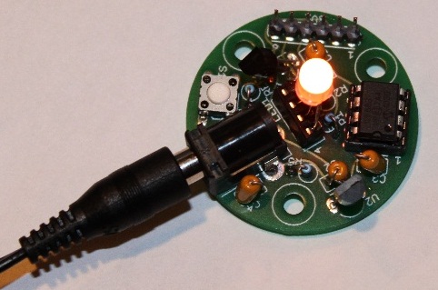
Temperature Candle Using LED

LED based projects require a lot of skill and hence only experienced circuit designers try out these circuits. But there are also a few circuits in this genre that can be done by amateur electronic hobbyists. The temperature candle is one such circuit. Read on to know more about this.

Hacks and Mods: Temperature Candle Using LED

The hardware components that are required to build this circuit are listed below:
  • Microcontroller
  • Temperature Sensor
  • RGB LED
  • PCB

The circuit design is pretty simple. The LED is made to flicker by the microcontroller and the color is based on the ambient temperature at that point. The temperature of the room can be known by observing the color of the LED.

The temperature value is obtained in degree Celsius. This value is received as a result of pressing the reset button on the PCB. This value can also be obtained by providing power to the device. Once the device is powered up, the change in temperature is indicated. The blue LED is triggered for a temperature increase of 10 degrees. The red LED is triggered for a temperature increase of a single degree.
Suppose, the ambient temperature is 23 degrees celsius, The circuit works in such a way that the blue LED is made to blink twice and the red LED is made to blink 3 times. Soon after this, an orange colored flicker is observed as the LED goes into canfle mode.

Since through hole components are used in this circuit, it is very cheap to construct and the components can be easily soldered. The circuit also contains a jack for connecting to a Microchip Pickit 3 programmer / debugger. This reduces the complexity involved in code modification and download.
Read more

Megaphone Circuit Diagram

This is a very simple loudspeaker amplifier which uses as an IC LM386, which is one of the most versatile amplifiers exists. The LM386, an operational amplifier receives the signal of MIC1 is a microphone which amplifies it and sends it to SPKR1 which is an 8-ohm speaker mounted in a cone to further amplify the audio signal.

Megaphone Circuit Diagram


Megaphone Circuit Diagram

Read more

Dual White Noise and Pink Noise Generator Circuit Diagram

This is a generator circuit which is very useful, it simultaneously generates two types of noise, pink and white. The noise generator is a circuit that produces electrical noise. Noise generators are used to test, measure noise, frequency response, and other parameters. The circuit described here is based on the operational amplifier 741.

 Dual White Noise and Pink Noise Generator Circuit Diagram

Dual White Noise and Pink Noise Generator Circuit Diagram
Read more

Small Audio Amplifiers Using LM386 and NE5534

Many electronic projects require the use of a small audio amplifier. Be it a radio transceiver, a digital voice recorder, or an intercom, they all call for an audio amp that is small, cheap, and has enough power to provide adequate loudness to fill a room, without pretending to serve a disco! About one Watt RMS seems to be a convenient size, and this is also about the highest power that a simple amplifier fed from 12V can put into an 8 Ohm speaker. A very low saturation amplifier may go as high up as 2 Watt, but any higher power requires the use of a higher voltage power supply, lower speaker impedance, a bridge circuit, or a combination of those.

During my many years building electronic things I have needed small audio amps many times, and have pretty much standardized on a few IC solutions, first and and foremost the LM386, which is small, cheap, and very easy to use. But it does not produce high quality audio... For many applications, the advantages weigh more than the distortion and noise of this chip, so that I used it anyway. In other cases I used different chips, which perform better but need more complex circuits. Often these chips were no longer available the next time I needed a small amplifier.

When I last upgraded my computer, I replaced the old and trusty Soundblaster AWE 32 by a Soundblaster Audigy. The new card is better in many regards, but while the old one had an internal audio power amplifier, the new one doesnt! Thats bad news, because I have some pretty decent speakers for the PC, which are fully passive. So, I built a little stereo amp using two LM386 chips and installed it inside the computer, fed by the 12V available internally.

But then I wasnt satisfied. The LM386 might be suitable for "communication quality" audio, which is roughly the fidelity you get over a telephone, but for music its pretty poor! The distortion was awful. So, the day came when I decided to play a little more scientifically with small audio amps, looking for a way to get good performance with simple and inexpensive means.

I set up a test bench with a sine wave oscillator running at 1 kHz, an 8 Ohm speaker, 12V power supply, and the computer with the soundcard and Fast Fourier Transform software. One channel was connected to the oscillator together with the amplifier input, the other channel to the output and speaker. With this setup I measured the harmonic content of the audio signals. I did the tests at an output level of 0.1W, which is typical for moderately loud sound from a reasonably efficient speaker. Also, I used a music signal from a CD player to test the actual sound of each amplifier.

Circuit Project: Small Audio Amplifiers Using LM386 and NE5534

As already said above, the main attraction of the LM386 is the extreme simplicity of its application circuit. You can even eliminate R1 if the signal source is DC-grounded. If the speaker leads are long, you should add an RC snubber across the output to aid stability. Additionally, if you need higher gain (not necessary if the input is at line level), you can connect a 10uF capacitor between pins 1 and 8. Thats about all there is to it.

Now the bad news: This circuit produced a very high level of distortion! The second harmonic measured just -28dB from the main output. The third harmonic was at -35dB, while the noise level was at -82dB. There were assorted high harmonics at roughly -45dB. With music, the distortion was really disturbing, and also the noise level was uncomfortably high. The power supply rejection is poor, so that some hum and other supply noise gets through. In short, this was a lousy performance!

Since I had used so many LM386s in my projects, I had several different variations. In my material box I found a slightly newer LM386N-1. So I plugged it into my test amplifier. It was even worse! The second harmonic was at -24dB, the third harmonic at -31dB, while the noise was a tad better at -84dB. Folks, thats a total harmonic distortion of almost 7%! And the 0.1W output level at which this was measured is where such a circuit is about at its best...  The distortion can be plainly seen on the oscilloscope, and a visibly distorted waveform is about the most offending thing an audio designer can ever see!

Looking through my projects, I found one where I had used a GL386 chip. This is just a 386 made by another company. I unsoldered it and put it in my test amplifier. Surprise! It was dramatically better, with the second harmonic at -45dB, and the third at -57dB! The noise floor was -84dB, just like the LM386N-1. But even this level of distortion was plainly audible when listening to music. Thats roughly 0.6% THD. Some folks may consider it acceptable for music. I dont, but for communication equipment its fine. At this point, I decided to see if I could build a better amplifier, that doesnt become too complex nor expensive.

Circuit Project: Small Audio Amplifiers Using LM386 and NE5534

This was the first attempt. A low distortion, fast slew rate, but easy to find and rather inexpensive operational amplifier, driving a simple source follower made of two small transistors. These transistors are not biased, so they work at zero quiescent current, in full class B. The only mechanism that works against crossover distortion here is the high slew rate of the OpAmp, which is able to make the distortion bursts during crossover very short. To say the truth, I didnt expect to get usable performance from this circuit, and was really surprised when it worked much better than the 386! The second harmonic was at -77dB, the third at -79dB!

Also there were many high harmonics at roughly -84dB. That means a THD of about 0.015%.  The noise floor was down at the -120dB level! The power supply rejection was excellent, with no detectable feedtrough. Playing music, this amplifier sounded really good: No audible noise, and the distortion could be heard when paying attention to it, but I doubt that the average person would detect it! Not bad, for a bias-less design!

Just to see how important the slew rate of the OpAmp is, I pulled out the NE5534 and replaced it by a humble 741, which is many times slower. The result was dramatic: The second harmonic still good at -70dB, but the third harmonic was much worse, at -48dB. Also there were many high harmonics at the same -48dB level. Given that second harmonic distortion doesnt sound bad to most people, but third harmonic does, and high harmonics are even worse, it came as no surprise that the amplifier with the 741 sounded bad.

At low volume it sounded particularly bad! So I returned to the oscillator and measurement setup, testing at lower output power, and found that while the second and third harmonics followed the output, the high harmonics stayed mostly constant! So, at very low output, the high harmonics became very strong relative to the output. All this is the effect of the slower slew rate of the 741, which makes it less effective correcting the crossover distortion of the unbiased transistors. Interestingly, the noise floor of the 741 circuit wasnt bad: -118dB.

Just for fun, I tried this circuit with a third OpAmp: The TL071, which is good, but not as good as the 5534. The results: Second harmonic at -72dB, third and the high ones at -60dB, and the noise at -120dB. Its interesting that the second harmonic is much more suppressed than the third one. That must be a balancing effect of the symmetric output stage, and the better symmetry in the TL071 compared to other OpAmps.

Its worthwhile to note that this amplifier can be simplified a lot by using a split power supply. R1, R2, C1, C2 and C4 would be eliminated! But then you need the capacitor removed from C4 to bypass the negative supply line. The positive input of the chip goes to ground, while pin 4 and the collector of Q2 go to the negative supply. The rest stays the same. If you use a +-15V supply, the available RMS output power grows to over 10 Watt! Of course, you then need larger transistors. And since larger transistors are slower, the distortion will rise somewhat. An added benefit of a split supply is that the popping noise when switching on and off is eliminated.

Circuit Project: Small Audio Amplifiers Using LM386 and NE5534

As the next experiment, I decided to get rid of the crossover distortion. For this purpose, I added a traditional adjustable bias circuit with a transistor and a trimpot. Now I also had to add a current source, because with the bias circuit there is no single point into which the OpAmp could put its drive current into both bases! I adjusted the bias for the best distortion, and this was really  a good one! The second harmonic was down right where the test oscillator delivered it, about -80dB, so I couldnt really measure it!

The third harmonic was at -84dB, and the best improvement was that the higher harmonics had simply disappeared! They were all below the noise floor, which stayed at -120dB. Actually, this noise floor seems to come from the soundcard A/D converter, so that the actual noise of this and the above amplifier may even be better! With music, this amplifier sounded perfect - clean and smooth. And Im pretty confident that the THD is well below the limits of my measurement setup, which is 0.01%.

The quiescent current was around 10mA. When lowering it to about 3mA, the high harmonics started to rise out of the noise floor. If you want to adjust the bias for the exact best quiescent current, there is a simple trick: Lift R4 from the output, and connect it to pin 6. Now the output stage has been left outside the feedback loop, and all its distortion will show up at the output. Watching the signal on an oscilloscope, or even better on a real time spectrum analyzer (soundcard and software), adjust the trimpot to the lowest distortion level.

Have a current meter in the supply line and make sure that you dont exceed 30mA or so of quiescent current, in order to keep the small transistors cool. But most likely the best distortion will be at a current lower than that. Once the adjustment is complete, return R4 to its normal position. Now the full gain and slew rate of the operational amplifier is used to correct the small remaining cross-over distortion of the output stage, and the distortion will certainly disappear from the scope screen, from your ears, and possibly fall below the detection level of the spectrum analyzer!

This circuit can also be run from a split power supply, by exactly the same mods as for the previous circuit. And since the transistors are properly biased, there isnt any significant distortion increase when using larger transistors. Be sure to use some that have enough gain - you have only a few mA of driving available, and with a +-15V power supply and an 8 Ohm speaker, there can be almost 2A of output current! So, you need a gain of 300 at least. There are power transistors in the 4A class that provide such gain, and these are good candidates. The other option is using Darlington transistors, which far exceed the gain needed here. But they will again increase the distortion, not very much, but perhaps enough to make it audible again.
 
 
Source: Humo Luden
Read more