This is the Simple Low Distortion Audio Amplifier Circuit Diagram. The circuit was designed and sold as a card by a purveyor of surplus components but, even using mostly manufacturers rejected transistors, we managed to get about 0.02% total harmonic distortion at 30 watts with a ±25v power supply into 8 ohms.: no bad figure even in these days of MOSFET and ICs. In 1977 anything below 0.1% was considered excellent. And this figure was pretty repeatable without doing much selection.
The problem of course is that since I havent touched this amplifier for many a year I have absolutely no idea what modern transistor types one should use for it but they are not critical: output transistors and drivers need to be the correct type but the other transistors can be small signal types - as long as they can handle the full voltage between + and - supplies.
Tr1 and Tr2 are a long-tailed pair (LTP to save typing). It is quite common to have a LTP in an audio amp but this is different: this is a complimentary LTP. As far as I am aware no one else had used a complimentary LTP at the time, though I have since seen it used in one other circuit. So I guess the circuit is unique to the author. One of the things that limits the performance of a conventional LTP is that the tail source loads the common emitters. In a complementary LTP this cant happen as there is no tail current source so that all the current of one transistor has to flow through the other.
Tr2s collector current flows into D1 and D2 which develop a voltage: this is used to bias Tr8 as a constant current source for Tr4s collector. The fact that Tr4 is working at a constant current defines its base-emitter voltage which must be developed across R4. This defines a current in R4 and this is the current that the LTP must operate at - so the ring of four transistors (Tr1, 2, 3, & 4) is self biasing and all transistors work at their best with minimum unwanted loads and biasing detracting from the performance. Tr4 is actually one of the most critical transistors: in the original circuit it was selected for Vce greater than 75v. Most Texas BC212s passed easily. Lower voltage transistors caused an increase in distortion level.
There is always a down side to any circuit: in the conventional LTP the base-emitter voltages tend to cancel each other out. In the complimentary LTP they add so there is a drop of about 1.2v between the two bases: this must be cancelled in the biasing chain and, since this circuit was designed for operation over a wide range of supply voltage, I had to be a little clever. Because of the constant current operation of the LTP and the constant voltage drop across D1 & D2, there is also a constant voltage across R14. This drop is used to lift up the bottom of the biasing chain (R1 and R11) so that the output sits at around half supply voltage, over a wider supply range.
D3 and D4 develop a bias voltage so that the output transistors are at the correct point, slightly conducting, to minimise crossover distortion.
The output transistors are complimentary (the original design used MJE2011 and MJE2021) and are driven by complimentary drivers: PNP driving NPN and vice versa. This arrangement is not only pleasingly symmetrical but gives better performance that the more common Darlington arrangement - the full gain of all the transistors is used and there is more internal feedback and less voltage drop.
The output current is monitored in the two resistors R7 and R22 (180 milliohms). The current limiting is unusual in that it works inside the input ring at an earlier stage than normal. This has an advantage that the current limiting transistors do not load the drive circuitry - which will introduce distortion. The slight down side is that there may be a slight tendency to oscillation when in current limit. R3 and R14 are necessary to restrict the current availability when the current limit engages. R5 and R19 are present to make the current limit vary with the voltage across the power transistors to avoid the second breakdown region of power transistors.
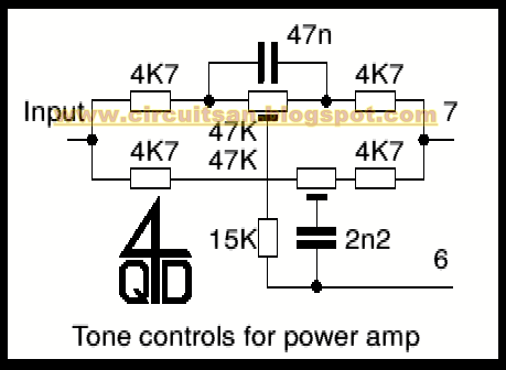
The points shown connecting terminals 1-2 and 6-7 are scratch-through tracks. 1 and 2 are the power and signal earths: to keep distortion in a stereo system to a minimum the currents in these must never share the same path so in a stereo system four earth wires are run to the systems common earth point - a spider common earth - and this means breaking the link. The link between 6 & 7 is in the feedback path and there are times when this can usefully be broken - one cheapskate was to fit a tone control circuit here (see below). It works fine but is a bit of an insult to such a low-distortion design!. A third break point is in the collector of Tr2. Breaking this shuts down the amplifier completely and safely. Is a thermal switch is to be fitted, this is the place.
Overall negative feedback is in two parts: D.c. is fed back via R13: there is 100% d.c. feedback. A.c. feedback is via R12 and R17. Note the output capacitor is inside this feedback loop (speaker connects between terminal 5 and negative) which extends the low frequency response.
Another feature is the accessibility of both ends of the output coupling capacitor: being designed for a junk shop, they didnt want to use expensive capacitors! So for extra bass performance an additional capacitor can easily be connected.
The circuit can also be driven as a low input impedance: break 6-7, short pin 8 to C4s positive and apply input to pin 6. In this mode the input distortion is actually better: my original notes show as low as 0.01%!
When building a low-distortion amplifier, layout is vital. In fact to get distortion around 0.02% requires a lot of skill and experience. The problem is that the current in the output stage alternates between the two power transistors so is a rectified version of the input. Now there is no such thing as a wire. Any real piece of wire or copper track is a resistor with associated inductance and capacitance. If the high current, rectified output signal mixes in the same piece of wire with the input signal the distortion in the rectified output current will feed into the input and cause the overall distortion to rocket. This is something which cannot properly be taught but has to be experienced. A skilled audio engineer will spend his lifetime learning about it.
Another interesting idea which is not shown is to fit a resistor between pin 3 and R18. This decreases the current at higher voltages and allows it to increase at low supply voltages. My notes show that this had a considerable advantage for low voltage operation because it increases the bias. It also is positive feedback which increase the open-loop voltage gain. It never got incorporated and I dont remember the details.
Tone controls
The circuit shows a simple (but effective) way of adding tone controls around the power amp. This does increase the distortion a little so it is not as hi-fi a solution as a separate tone control stage, but it is simple and quite effective.
To use the tone controls you must break the link between 6 and 7 on the circuit. Also the 150K resistor, R13, should be decoupled. Replace it by two 68K resistors in series. The centre point of these two connects to the positive of a 1µ electrolytic whose negative connects to the earth (0v) line. This stops R13 acting as negative feedback which otherwise would shunt the tone controls.
Sourced by : Author: Richard Torrens
Site hosted by Arachsys


 R1=15k