Thursday, November 20, 2014

Sine Wave To TTL Converter

Sine Wave To TTL Converter is a series that we can use to change the sine wave signal with a pulse shape with the same frequency with TTL logic level that we are ready to use in coding the data digitally . The series of Sine Wave To TTL Converter can be used to convert sine wave signal to form a TTL of frequency 100KHz to 80MHz at the level of 100mV - 2V. The series of Sine Wave To TTL Converter uses a 5VDC voltage source. The series of Sine Wave To TTL Converter was built from transistor T1 gets base bias from R3, R4 and R5. If the series Sine Wave Converter This TTL To get the input sine signal with a minimum level of 100mV, the circuit Sine Wave To TTL Converter This will generate an output signal with TTL level square wave.

The series of Sine Wave To TTL Converter has input + impedance - 50 Ohm which is set using the R6. To change the value of the input impedance converter circuit Sine Wave To this TTL can be set via the R6 with a maximum value of 300 ohms.
Read more

Wednesday, November 19, 2014

Transistor As a timer circuit

Basically on all timer or timer circuit utilizing most of the basic characteristics of the capacitor.

Transistor

 The basic characteristic is the process of filling and discharge that occurs in the capacitor. The length of time charging and release depends on the value of the capacitor.

If we observe the above circuit, the light will immediately switch SW1 turns on when we plug it into potensio VR1, this is because the current flowing from VR1 to trigger the transistor base should fill the first capacitor C1. Semakian large capacitance value of C1 then the longer the time required by the transistor to turn on the lights. Then if we connect it to the Ground SW1 then light would soon die and the capacitor will immediately clear the cargo. So can we draw the conclusion that the transistor can be used as a timer circuit using capacitor charging and discharging properties.
Read more

Audio Power Amplifier LM3886

Audio Power Amplifier is an important part in the reproduction of sound in a sound system. Audio Power Amplifier LM 3886 with power IC Audio Power Amplifier is a highly capable and able to produce 68 Watts with power rata2 4Ohm load and capable of producing power 38 Watt with 8Ohm load. With good sound reproduction capabilities of 20Hz-20kHz is also included on this LM3886 Audio Power Amplifier. LM3886 Audio Power Amplifier is equipped with spike protection that will protect the output circuit from overvoltage, undervoltage, overloads, konrsleting power supply, thermal runawaydan peak temperature. Audio Power Amplifier LM3886 also features a noise reduction system which can keep the audio from the noise well.

Image of Basic Audio Power Amplifier Series LM3886

Audio


Audio Power Amplifier LM3886

Feature owned LM3886 Audio Power Amplifier

  • 68W cont. avg. output power into 4Ω at VCC = ± 28V
  • 38W cont. avg. output power into 8Ω at VCC = ± 28V
  • 50W cont. avg. output power into 8Ω at VCC = ± 35V
  • 135W instantaneous peak output power capability
  • Signal-to-Noise Ratio ≥ 92dB
  • An input mute function
  • Output protection from a short to ground or to the supplies via internal current limiting circuitry
  • Output over-voltage protection against transients from inductive loads
  • Supply under-voltage protection, not allowing internal biasing to occur Pls | VEE | + | VCC | ≤ 12V, Thus eliminating turn-on and turn-off transients
  • 11-lead TO-220 package
  • Wide supply range 20V - 94V
  • Application of Audio Power Amplifier LM3886
  • Stereo audio system
  • Active Speaker
  • High End Audio Power TV
  • Suround Power Amplifier
Read more

Tuesday, November 18, 2014

1000 Watt Power Amplifier

Power amplifier has up to 1000 Watt power, this circuit made one channel only so if you want to create a stereo in it must be made one again, actually this is more suitable power amplifier in use for Sound System or outdoor, so if only in use for the house I think is less suitable.
Maybe youve seen or even have an active speaker and there is written 1500 watts PMPO (Peak Music Power Output), make no mistake this is different from Power Amplifier Active Speaker, I often dismantle such Active Speaker in it only a power with power no more than 150 watts by using the transformer 2-3 Ampere. PMPO is not a real power which is issued by the Power Amplifier, but counting all the speakers that there is, for example: if there are 5 pieces of speakers on each channel and each speaker has a power of 10 W then it is 100 W PMPO.
1000W Power Amplifier schematics
Part List 1000W amplifier
While this 1000 Watt Power Amplifier minimal use transformer 20 Ampere. And the output of Power Amplifier DC voltage contains approximately 63 volts, with currents and voltages of this magnitude, this 1000 Watt Power Amplifier will not hesitate hesitate to destroy your woofer speakers to connect. To overcome that then before the speaker on connects to 1000 Watt Power Amplifier must be in pairs Speaker Protector.

Actually if you want to create a Power Amplifier with great power does not have to make a Power Amplifier with great power. Example: you want to create a Power Amplifier with 10 000 Watt power. You do not have to assemble a Power Amplifier with power of 10,000 watts, but you assemble the power Power Amplifier Small but many, such as you assemble the Power Amplifier with 1000 Watts of power for as many as 10 pieces, it will produce 10 000 Watt Power Amplifier helpless.

Circuit uses power transistors pair of 5 x 5 x 2SA1216 and 2SC2922 and 2SC1583 use a differential amplifier that actually contains 2 pieces of transistors that are in containers together. Why use such built-in amplifier differental tujuanya so identical / similar, could have uses 2 separate transistors but can result in amplifier so it is not symmetrical.

Tips combining speaker.

To get the speakers with great power combining techniques can be used in parallel series, combining each group of speakers should sepaker they will have the same impedance, the same type (Woofer, Mid Range or tweeter) and the same power. Number of merging these speakers should consists of 4 , 9, 16 ff, see picture
Speaker wiring


Example: The number of speakers have 4 pieces each of its 200 Watt power generated will be a speaker at = 200 x 4 = 800 Watt. If there are 9 speakers 200 W then the result = 9 x 200 W = 1800 Watt.
Read more

Subwoofer power amplifier IC OPA541BM

Subwoofer power amplifier circuit based on IC OPA541BM very suitable for use in subwoofer speakers, these amplifiers possess excellence in sound issud because the sound is very clear and issued in accordance with subwoofer speakers in a low tone.
Subwoofer power amplifier IC OPA541BM Circuit

Read more

Monday, November 17, 2014

LM4651 and LM4652 170W power amplifier

170 Watt power amplifier is a power amplifier that is built by IC LM4651 and LM4652. Part of this power amplifier driver using the LM4651 IC designed specifically for the purpose of the class AB amplifier driver with short circuit protection feature, containing under voltage, thermal shutdown protection and standby functions. Section 170 Watt power amplifier using LM4651 IC with a MOSFET power amplifier is equipped with temperature sensors that will be used by IC LM4651 as controlnya thermal signal. IC IC LM4651 and LM4652 are designed specifically to each other in pairs to create a class AB power amplifier with protection features are detailed. Detailed series of 170 Watt power amplifier can be seen in thethe following figure .

LM4651

Power amplifier circuit requires supply voltages +22 V DC symmetrical 0-22V. Power Amplifier with IC LM4651 and LM4652 are often used in portable HiFi systems such as powered speakers, power subwoofer and car audio power Booter. D1, D2, D3 and D4 in series 170 watt power amplifier with LM4651 and LM4652 is a 22V zener diode.
Read more

Vertical IC Configuration

Various kinds of vertical out IC configuration.Ac coupling -connect from the yoke deflection output to a coil connected directly.Dc coupling - connected the output to the coil through a capacitor deflectioan yoke. Electrolityc Capacitors (usually worth 1000u/35v). This configuration requires two kinds of voltage (the voltage mirror plus-minus).Dc input coupling using diffferential - uses 2 input from the driver IC.

Vertical IC Configuration AC Coupling

Vertical IC Configuration DC Coupling

Read more

Sunday, November 16, 2014

PWM Motor Controller

PWM Motor Controller With Forward And Reverse is circuit controllers for DC motors controlled by PWM technique . The series PWM Motor Controller With Forward And Reverse It can control the DC motor rotation direction. Speed ​​control by PWM technique through MOSFETs Q1 IRF150. Then to play with the directional control relay which is controlled by Q10 using control signals in the form of logic 0 and 1. The series PWM Motor Controller With Forward And Reverse It requires 12 VDC supply voltage.
Circuit PWM Motor Controller With Forward And Reverse the above can be used to control large DC motor with maximum current consumption 10A.
Read more

Saturday, November 15, 2014

METAL DETECTOR CIRCUIT

Metal detector is very common devices for checking the person in shopping malls, hotels, cinema halls to ensure that person is not carrying any explosive metals or illegal things like guns, bombs etc. metal detectors can be created easily and the circuit is not that complex.


Block Diagram
The LC circuit is nothing but inductor and capacitor which is connecter in parallel. The LC circuit will trigger the proximity sensor if it detects any metal near to it. Proximity sensor will give glow the led, and also make the buzz with the help of the buzzer.

Main Components in Metal Detector Circuit

LC CIRCUIT : LC Circuit is a resonating circuit which will resonate when exact same frequency material comes near. The LC circuit consist of inductor and capacitor connected in parallel , when the capacitor is fully charged the charge of the capacitor will be given to the inductor, here inductor will have improve its magnetic field. After some time the capacitor will have no charge and current from the inductor will be given to the capacitor in a reverse polarity and capacitor will get charge and now the inductor magnetic field and current will become nil. Again charged capacitor will give current to the inductor to improve its magnetic field. Note inductor is a magnetic field storage device and capacitor is electric field storage device.

PROXIMTY SENSOR : The proximity sensor can detect the objects with out any physical interference. The proximity sensor will work same as infrared sensor, proximity also release a signal, it will not give output unless and until there is no change in the reflected back signal, If there is a change in signal it will detect and give the output accordingly. There are different proximity sensors for example to detect plastic material we can use capacitive type proximity and for metals we should use inductive type.

Circuit Diagram


Circuit Working

  • When the LC circuit that is L1 and C1 has got any resonating frequency from any metal which is near to it, electric field will be created which will lead to induces current in the coil and changes in the signal flow through the coil.
  • Variable resistor is used to change the proximity sensor value equal to the LC circuit, it is better to check the value when there is coil not near to the metal. When the metal is detected the LC circuit will have changed signal. The changed signal is given to the proximity detector (TDA 0161), which will detect the change in the signal and react accordingly. The output of the proximity sensor will be of 1mA when there is no metal detected and it will be around 10mA when coil is near to the metal
  • When the output pin is high the resistor R3 will provide positive voltage to transistor Q1. Q1 will be turned on and led will glow and buzzer will give the buzz. Resistor r2 is used to limit the current flow.
Read more

Friday, November 14, 2014

Digital to Analog Converter using Binary Weighted Resistors R 2R

The R-2R ladder DAC which is a binary-weighted DAC that uses a repeating cascaded structure of resistor values R and 2R. This improves the precision due to the relative ease of producing equal valued-matched resistors (or current sources). However, wide converters perform slowly due to increasingly large RC-constants for each added R-2R link. The D/A converter using binary-weighted resistors is shown in the figure below. In the circuit, the op-amp is connected in the inverting mode. The op-amp can also be connected in the non-inverting mode. The circuit diagram represents a 4-digit converter. Thus, the number of binary inputs is four.

Circuit Diagram


Fig. 1
We know that, a 4-bit converter will have 24 = 16 combinations of output. Thus, a corresponding 16 outputs of analog will also be present for the binary inputs.

Four switches from b0 to b3 are available to simulate the binary inputs: in practice, a 4-bit binary counter such as a 7493 can also be used.

Working

The circuit is basically working as a current to voltage converter.

1. b0 is closed
It will be connected directly  to the +5V.
Thus, voltage across R = 5V
Current through R = 5V/10kohm = 0.5mA
Current through feedback resistor, Rf = 0.5mA (Since, Input bias current, IB is negligible)
Thus, output voltage = -(1kohm)*(0.5mA) = -0.5V

2. b1 is closed, b0 is open
R/2 will be connected to the positive supply of the +5V.
Current through R will become twice the value of current (1mA) to flow through Rf.
Thus, output voltage also doubles.

3. b0 and b1 are closed
Current through Rf = 1.5mA
Output voltage = -(1kohm)*(1.5mA) = -1.5V

Thus, according to the position (ON/OFF) of the switches (bo-b3), the corresponding “binary-weighted” currents will be obtained in the input resistor. The current through Rf will be the sum of these currents. This overall current is then converted to its proportional output voltage. Naturally, the output will be maximum if the switches (b0-b3) are closed,

V0 = -Rf *([b0/R][b1/(R/2)][b2/(R/4)][b3/(R/8)]) 
Where each of the inputs b3, b2, b1, and b0 may either be HIGH (+5V) or LOW (0V).

The graph with the analog outputs versus possible combinations of inputs is shown below.

Fig. 2
The output is a negative going staircase waveform with 15 steps of -).5V each. In practice, due to the variations in the logic HIGH voltage levels, all the steps will not have the same size. The value of the feedback resistor Rf changes the size of the steps. Thus, a desired size for a step can be obtained by connecting the appropriate feedback resistor. The only condition to look out for is that the maximum output voltage should not exceed the saturation levels of the op-amp. Metal-film resistors are more preferred for obtaining accurate outputs.

Disadvantages

If the number of inputs (>4) or combinations (>16) is more, the binary-weighted resistors may not be readily available. This is why; R and 2R method is more preferred as it requires only two sets of precision resistance values.

Read more

Thursday, November 13, 2014

LM390 Simple 2 Way intercom Circuit

This is a very simple two way intercom circuit based on a LM390 audio amplifier circuit . the intercom circuit is a stand-alone electronic communications system intended for limited or private dialogue. For this circuit you can use a 8 ohms speaker, one for each station and require a 6 volts dc power supply. Gain control can be done by capacitively coupling a resistor (or FET) from pin 6 to ground.

LM390 Simple 2-Way intercom Circuit
LM390 Pin out

The LM390 Power Audio Amplifier is optimized for 6V, 7.5V, 9V operation into low impedance loads. The gain is internally set at 20 to keep the external part count low, but the addition of an external resistor and capacitor between pins 2 and 6 wil increase the gain to any value up to 200. The inputs are ground referenced while the output is automatically biased to one half the supply voltage.
Read more

Transistor Schmitt Trigger Oscillator

The Schmitt Trigger oscillator below employs 3 transistors, 6 resistors and a capacitor to generate a square waveform. Pulse waveforms can be generated with an additional diode and resistor (R6). Q1 and Q2 are connected with a common emitter resistor (R1) so that the conduction of one transistor causes the other to turn off. Q3 is controlled by Q2 and provides the squarewave output from the collector.


In operation, the timing capacitor charges and discharges through the feedback resistor (Rf) toward the output voltage. When the capacitor voltage rises above the base voltage at Q2, Q1 begins to conduct, causing Q2 and Q3 to turn off, and the output voltage to fall to 0. This in turn produces a lower voltage at the base of Q2 and causes the capacitor to begin discharging toward 0. When the capacitor voltages falls below the base voltage at Q2, Q1 will turn off causing Q2 and Q3 to turn on and the output to rise to near the supply voltage and the capacitor to begin charging and repeating the cycle. The switching levels are established by R2,R4 and R5. When the output is high, the voltage at the base of Q2 is determined by R4 in parallel with R5 and the combination in series with R2. When the output is low, the base voltage is set by R4 in parallel with R2 and the combination in series with R5. This assumes R3 is a small value compared to R2. The switching levels will be about 1/3 and 2/3 of the supply voltage if the three resistors are equal (R2,R4,R5).

There are many different combinations of resistor values that can be used. R3 should low enough to pull the output signal down as far as needed when the circuit is connected to a load. So if the load draws 1mA and the low voltage needed is 0.5 volts, R3 would be 0.5/.001 = 500 ohms (510 standard). When the output is high, Q3 will supply current to the load and also current through R3. If 10 mA is needed for the load and the supply voltage is 12, the transistor current will be 24 mA for R3 plus 10 mA to the load = 34 mA total. Assuming a minimum transistor gain of 20, the collector current for Q2 and base current for Q3 will be 34/20 = 1.7 mA. If the switching levels are 1/3 and 2/3 of the supply (12 volts) then the high level emitter voltage for Q1 and Q2 will be about 7 volts, so the emitter resistor (R1) will be 7/0.0017 = 3.9K standard. A lower value (1 or 2K) would also work and provide a little more base drive to Q3 than needed. The remaining resistors R2, R4, R5 can be about 10 times the value of R1, or something around 39K.

The combination of the capacitor and the feedback resistor (Rf) determines the frequency. If the switching levels are 1/3 and 2/3 of the supply, the half cycle time interval will be about 0.693*Rf*C which is similar to the 555 timer formula. The unit I assembled uses a 56K and 0.1 uF cap for a positive time interval of about 3.5 mS. An additional 22K resistor and diode were used in parallel with the 56K to reduce the negative time interval to about 1 mS.

In the diagram, T1 represents the time at which the capacitor voltage has fallen to the lower trigger potential (4 volts at the base of Q2) and caused Q1 to switch off and Q2 and Q3 to switch on. T2 represents the next event when the capacitor voltage has risen to 8 volts causing Q2 an Q3 to turn off and Q1 to conduct. T3 represents the same condition as T1 where the cycle begins to repeat. Now, if you look close on a scope, you will notice the duty cycle is not exactly 50% This is due to the small base current of Q1 which is supplied by the capacitor. As the capacitor charges, the E/B of Q1 is reverse biased and the base does not draw any current from the capacitor so the charge time is slightly longer than the discharge. This problem can be compensated for with an additional diode and resistor as shown (R6) with the diode turned around the other way. 
Read more

Wednesday, November 12, 2014

Simple 2 1 Surround Speaker System Circuit Diagram

 "Simple 2.1 Surround Speaker System " . Here I have used  three TDA 2030 IC for making signal amplification . Here you need a sub filter extra ( Sub filter circuit diagram link showing below ) . This project  mostly used in computer  . Part list and applications are showing below.

Part List
Component No:ValueUsage
All C1100MF Grounding 
All C2100nFGrounding
All C3100nFGrounding
All C4100MFGrounding
All C5100MFFeedback
All C6100MFAudio Coupling 
All C7220nFNoise Grounding 
All R11K
All R210K ( Not 1K )
All R322K
All R422K (Not 1K )
All RV1100KVolume Controlling 
All D1 To D2IN4007Potential Breaking
U1 To U6TDA2030Amplification

Applications* 2.1 Surround Amplifier

* 2.1 Home Theater
Read more

Wireless Microphone simple

 wireless microphone sederhana


  Wireless Microphone simple Parts list:

* T1,T2,T3: 2N2222 transistor
* R1: 10k 5%
* R2: 33k lin.
* R3: 12k 5%
* R4: 5.6k 5%
* R5: 2.2k 5%
* R6,R8: 47k 5%
* R7: 470 ohms 5%
* R9: 180 ohms 5%
* C1,C2: 47nF
* C3: 1nF
* C4: 33pF
* C5: 5.6pF
* C6: 8.2pF
* C7: 10nf
* L1: 3mm in diameter with 5 turns 0.61 mm copper wire
* K1: SPDT toggle switch
* Other parts: 2 AA battery holder, Electret microphone, antenna wire

Wireless FM microphone is simple to body and it has a advantageous transmitting ambit (over 300 meters in the accessible air). Despite its baby basic calculation and a 3V operating voltage it will calmly access over three floors of an accommodation building. It may be acquainted anywhere in the FM bandage (87-108MHz) and its transmissions can be best up on any accepted FM receiver.

The braid (L1) should be about 3mm in bore with 5 turns 0.61 mm chestnut wire. You can alter the Tx abundance by artlessly adjusting the agreement of the coils. The antenna should be a bisected or division amicableness continued (for 100 MHz 150 cm or 75 cm).

Circuit description:The audio addition date (T1) is a accepted accepted emitter amplifier. The 47nF capacitor isolates the microphone from the abject voltage of the transistor and alone allows AC signals to pass.

The LC catchbasin ambit is complete with T2, the acknowledgment capacitor C5 and the alongside LC ambit L1, C4. The coupling capacitor(C6) directs the arresting to the RF amplifier (T3).

Circuit calibration: Place the transmitter about 10 anxiety from a FM radio. Set the radio to about about 89 – 90 MHz. Spread the ambagious of the L1 braid afar to tune to the adapted frequency.

Read more

Tuesday, November 11, 2014

Sunday, November 9, 2014

Simple Heat Sensor Circuit Diagram

This simple heat sensor circuit could senses heat from various electronics device like computer, amplifier etc. and generate warning alarm. It could senses heat from environment also, but here I mention “electronics device” because it is being using mostly in electronic device to protect them from overheat.

Thermistor, 110 Ohms:

Thermistor
Fig-2: 110 Ohms Thermistor
As it is a heat sensor circuit, here a thermistor is used as a heat sensor. It is a thermal measurement device and has a variety of usages including temperature sensor/ heat sensor. The thermistor used in this circuit is a NTC (Negative Temperature Coefficient) type thermistor. When temperature increases, its resistance goes decrease. Therefore, NTC thermistor’s resistances are inverse of temperature.

Circuit Description:

You have seen, in this simple circuit diagram of heat sensor, a few number of components is used including a BC548 transistor, a 110 ohms thermistor etc.
  • BC548: BC548 is a TO-92 type NPN transistor, as its alternative you can use 2N2222, BC238, BC548, BC168, BC183 etc. they all have almost same characteristic.
  • 110 Ohms Thermistor: A 110 Ohms thermistor is used to detecting heat. I have told already about it.
  • Buzzer: A buzzer is used with +9V and collector of transistor. When the temperature/ heat exceeds a certain level then it make an alarm.
  • 4.7V Zener diode:  It is used to limit the emitter current of BC548.
  • 9V Battery: A 9V battery is used as a single power source.
  • R1, R2: A 3.3K 1/4w resistor is used as R1 and 100 ohms 1/4w as R2.
  • Switch: Here in this circuit the switch used is a simple SPST switch. You can either use the switch or not, choice is yours. It is not mandatory.
Read more

Saturday, November 8, 2014

Car Head Lights Turn Off

This circuit when setup in a car automatically turns off the head light after a preset time after the ignition switch is turned off.So you can walk out easily from the dark garage in the light of your car.

Circuit diagram :


Car Head Lights Turn Off  Circuit Diagram
When the ignition switched on first the voltage from battery is fed to the relay through diode D1.When the ignition switch is turned off it produces a negative going pulse at the pin 2 that triggers the timer. The output of the IC goes high for the time set by R1  .This makes the transistor Q1 to conduct to energize the relay to drive the headlight.After the set time the light goes off.With the value of components used you can make a setting from 10 S to 60 S.
Notes :
  • Assemble the circuit on a good quality PCB or common board.
  • Fit the potentiometer on somewhere on the dashboard so that  you can easily set the timing.
Read more

Cheap Pump Controller

This simple but effective circuit can be used to control water level in a container. The prototype is used to pump water out of a bucket that collects condensation from a home air-conditioning system. The design is based around a 555 timer (IC1). Although the timer in configured as a mono-stable, it lacks the usual timing capacitor from pin 6 to ground. Instead, a metal probe inserted in the water provides a current path to a second, grounded probe. When the water level in the container reaches a third ("high") probe, the trigger input (pin 3) is pulled low, switching the 555 output high and energizing the relay via transistor Q1.


Cheap Pump Controller Circuit Diagram

Once the water level drops below the "low" probe, the threshold input (pin 6) swings high, switching the output (pin 3) low and the relay and pump off. The two 100kΩ pull-up resistors can be replaced with larger values if more sensitivity is required (eg, if the 555 doesn’t trigger). A switch (S1) can be included to bypass the relay for manual emptying. The "low" probe should be positioned so that the pump doesn’t run dry.


The high level probe is placed at the level that you want the pump to start. Since the water is held at ground potential, you must use stainless steel or copper wire to slow corrosion. With water fountain pumps available for less than $10, this circuit offers a cheap alternative for those who have an air-conditioner on an internal wall and don’t want to be continually emptying the bucket on humid days.
Read more

Thursday, November 6, 2014

Sound Activated Lights

This diy sound activated lights circuit turns a lamp ON for a short duration when the dog barks (or a relatively strong sound) giving an impression that the occupants have been alerted. The condenser microphone fitted in a place to monitor sound and generates AC signals, which pass through DC blocking capacitor C1 to the base of transistor BC549 (T1). Transistor T1 along with transistor T2 amplifies the sound signals and provides current pulses from the collector of T2. When sound is produced in front of the condenser mic, triac1 (BT136) fires, activates lights and the bulb (B1) glows for about two minutes.
Assemble the sound activated lights circuit on a general purpose PCB (circuit board) and enclose in a plastic cabinet. Power to the sound activated switch circuit can be derived from a 12V, 500mA step-down transformer with rectifier and smoothing capacitor. Solder the triac ensuring sufficient spacing between the pins to avoid short circuit. Fix the unit in the dog’s cage or close to the sound monitoring spot, with the lamp inside or outside as desired. Connect the microphone to the sount activated lights circuit using a short length of shielded wire. Enclose the microphone in a tube to increase its sensitivity.

Caution. Since the sound activated lights uses 230V AC, many of its points are at AC mains voltage. It could give you lethal shock if you are not careful. So if you don’t know much about working with line voltages, do not attempt to construct this circuit. We will not be responsible for any kind of resulting loss or damage.
Read more

Precision Headphone Amplifier

Designs for good-quality headphone amplifiers abound, but this one has a few special features that make it stand out from the crowd. We start with a reasonably conventional input stage in the form of a differential amplifier constructed from dual FET T2/T3. A particular point here is that in the drain of T3, where the amplified signal appears, we do not have a conventional current source or a simple resistor. T1 does indeed form a current source, but the signal is coupled out to the base of T5 not from the drain of T3 but from the source of T1. Notwithstanding the action of the current source this is a low impedance point for AC signals in the differential amplifier.  

Precision Headphone Amplifier Circuit Diagram


Measurements show that this trick by itself results in a reduction in harmonic distortion to considerably less than –80 dB (much less than 0.01 %) at 1 kHz. T5 is connected as an emitter follower and provides a low impedance drive to the gate of T6: the gate capacitance of HEXFETs is far from negligible. IC1, a volt-age regulator configured as a current sink, is in the load of T6. The quiescent current of 62 mA (determined by R11) is suitable for  an output power of 60 mWeff into an impedance of 32 Ω, a value typical of high-quality headphones, which provides plenty of volume.


Using higher-impedance headphones, say of 300 Ω, considerably more than 100 mW can be achieved. The gain is set to a useful 21 dB (a factor of 11) by the negative feedback circuit involving R10 and R8. It is not straightforward to change the gain because of the single-sided supply: this voltage divider also affects the operating point of the amplifier. The advantage is that excellent audio quality can be achieved even using a simple unregulated mains supply.  Given the relatively low power output the power supply is considerably overspecified. Noise and hum thus remain more than 90 dB below the signal (less than 0.003 %), and the supply can also power two amplifiers for stereo operation.

The bandwidth achievable with this design is from 5 Hz to 300 kHz into 300 Ω, with an output voltage of 10 Vpp. The damping factor is greater than 800 between 100 Hz and 10 kHz. A couple of further things to note: some-what better DC stability can be achieved by replacing D1 and D2 by low-current red LEDs (connected with the right polarity!). R12 prevents a click from the discharge of C6 when headphones are plugged in after power is applied. T6 and IC1 dissipate about 1.2 W of power each as heat, and so cooling is needed. For low impedance headphones the current through IC1 should be increased. To deliver 100 mW into 8 Ω, around 160 mA is required, and R11 will need to be 7.8 Ω (use two 15 Ω resistors in parallel).

To keep heat dissipation to a reasonable level, it is recommended to reduce the power supply volt-age to around 18 V (using a transformer with two 6 V secondaries). This also means an adjustment to the operating point of the amplifier: we will need about 9V between the positive end of C6 and ground. R4 should be changed to 100 Ω, and R8 to 680 Ω. The gain will now be approximately 6 (15 dB). The final dot on the ‘i’ is to increase C7 by connecting another 4700 µF electrolytic in parallel with it, since an 8 Ω load will draw higher currents.
Read more

Wednesday, November 5, 2014

Battery Equality Monitor

Almost all 24V power systems in trucks, 4WDs, RVs, boats, etc, employ two series-connected 12V lead-acid batteries. The charging system can only maintain the sum of the individual battery voltages. If one battery is failing, this circuit will light a LED. Hence impending battery problems can be forecast. The circuit works by detecting a voltage difference between the two series connected 12V batteries. Idle current is low enough to allow the unit to be permanently left across the batteries.

Battery Equality Monitor Circuit Diagram

battery_equality_monitor_schematic_circuit_diagramw

Parts:

R1 = 2.K
R2 = 4.7K
R3 = 39K
R4 = 39K
R5 = 1.5K
R6 = 1.5K
Q1 = BC547
Q2 = BC547
Q3 = BC557
D1 = 3mm Red LED
D2 = 3mm GreenLED
B1 = DC 12 Volt
B2 = DC 12 Volt

Read more

Automotive Voltage Indicator

Monitors battery voltage, Three-LED Display. Connecting this circuit to the battery of your vehicle, you will always know at a glance the approximate voltage available. An indication of battery voltage is useful to the motorist for monitoring the batterys capacity to deliver current, and as a check on the efficiency of the dynamo or alternator. Threshold voltages of the Leds are set by means of two Zener Diodes (D6 & D10) plus two further Diodes wired in series (D4, D5 and D8, D9 respectively) adding a step of about 1.3V to the nominal Zener voltage.

Automotive Voltage Indicator Circuit Diagram :

 indicator cicuit diagram
Parts:
R1 = 1k
R2 = 100K
R3 = 1k
R4 = 3.3K
R5 = 3.3K
R6 = 1k
R7 = 3.3K
R8 = 3.3K
Q1 = BC547
Q2 = BC547
Q3 = BC557
D1 = Red Led
D2 = Amber Led
D3 = 1N4148
D4 = 1N4148
D5 = 1N4148
D6 = BZX79C10
D7 = Green Led
D8 = 1N4148
D9 = 1N4148
D10 = BZX79C12

Notes:
  • Red LED D1 is on when battery voltage is 11.5V or less. This indicates a low battery charge.
  • Amber LED D2 is on when battery voltage is comprised in the 11.5 - 13.5V range. This indicates that the battery is good if the motor is off. When motor is running, this indicates no charge from dynamo or alternator.
  • Green LED D7 is on when battery voltage is 13.5V or more. This indicates a normal condition when motor is running and dynamo or alternator is charging.
Read more

Tuesday, November 4, 2014

Cable Tester

This cable tester allows you to quickly check audio cables for broken wires. Because of the low power supply voltage, batteries can be used which makes the circuit portable, and therefore can be used on location.

Cable Tester Circuit diagram:

Tester-Circuit

The design is very simple and well organ-ised: using the rotary switch, you select which conductor in the cable to test. The corresponding LED will light up as indication of the selected conductor. This is also an indication that the power supply volt-age is present. If there is a break in the cable, or a loose connection, a second LED will light up, corresponding to the selected conductor. You can also see immediately if there is an internal short circuit when other than the corresponding LEDs light up as well.

You can also test adapter and splitter cables because of the presence of the different connectors.
Two standard AA- or AAA- batteries are sufficient for the power supply. It is recommended to use good, low-current type LEDs. It is also a good idea not to use the cheapest brand of connectors, otherwise there can be doubt as to the location of the fault. Is it the cable or the connector.


Read more

Regulated 24 Watt Broad Spectrum LED

This project involves constructing an energy efficient broad spectrum LED lamp system. The lamp is useful for indoor reflective room lighting. It has a broad color spectrum that more closely approximates the light of the sun when compared to fluorescent bulbs and white-only LEDs. The light level is regulated and the light that is produced does not flicker.

The six differently colored LED stars, made by LedEngin, Inc., are rated at 5 watts (nominal). The LED array and associated current regulator consume 1 amp at 24VDC (24 Watts). NEVER stare directly at this lamp when it is running at full operating power, it is DANGEROUSLY BRIGHT.

Regulated 24 Watt Broad Spectrum LED Circuit diagram : 

24


With the LEDs shown, the combined color of the lamp has a pinkish white hue. The 5 Watt ratings of the LEDs are not precise, the white, blue and green LEDs consume about 4W and the lower voltage red, orange and deep red LEDs consume about 3W. The current regulator keeps the LED brightness constant and insures that the LED series string never draws more than 1 amp of current.

The project has also been coined "Bold as LED" in reference to the Jimi Hendrix song "Bold as Love" which has the lyric: "My yellow in this case is not so mellow"

Specifications:
  • Nominal operating power: 24 Watts (24V DC at 1 Amp)
  • LED power consumption above regulation point: 18.6 Watts
  • Maximum operating voltage: 28V DC
  • Minimum voltage for regulated light: 23V DC
  • Leds produce light down to 11V
  • Deep Red LED voltage: 2.55V
  • Red LED voltage: 2.37V
  • Amber LED voltage: 2.60V
  • Green LED voltage: 3.92V
  • Blue LED voltage: 3.56V
  • White LED voltage: 3.7V
  • Voltage across regulator when current becomes regulated: 4.2V

Theory:

The lamp is wired as a current loop which includes the power supply, the LED series string and the 1 amp current regulator circuit. The LM317K and 1.2 ohm 5 Watt resistor act as a current regulator that limits the loop current to 1 Amp. During regulation, there will always be 1.2V across the 1.2 ohm resistor. The current regulator insures that the LEDs always run at their maximum brightness, but not so bright that they burn out. A 100uF electrolytic capacitor bypasses the DC power input to the device and a 100nF monoblock capacitor bypasses the LM317K input.

Construction:

The LEDs and current regulator circuit were mounted on a 3" x 8" chunk of 1/8" aluminum stock. The LM317K regulator and LED heat sinks were bolted to the chassis directly, heat sink grease was used on the regulator, the heat sinks and the six LEDs. Connecting the LM317K directly to the aluminum plate makes the plate electrically hot at 1.2V, the plate should not be allowed to come into contact with any live conductors. By using a few more parts, the LM317 can be mounted with an insulator and plastic shoulder washers for electrical isolation from the mounting plate.

The LEDs come mounted on their own small star-shaped aluminum substrates, these were attached to the aluminum plate using two 7/16" 4-40 screws and nuts per LED. A drop of silicone heat sink grease should be applied to the center of each LED star when it is mounted to the plate for heat conduction. It is important to use insulating plastic washers on the top side of the LED stars to prevent electrical contact with head of the screw. The LED stars were soldered together using short pieces of #20 tinned wire after being mounted on the plate. It is necessary to use a fair amount of heat to solder the contacts, a 200/240W soldering gun did the job. Be very careful not to melt the lenses on the LEDs, the LEDs cost around $10 each. The positive and negative leads of the LED series string were connected back to the current reglator circuitry using #20 wire covered with teflon insulation.

The initial mechanical arrangement did not pass the "rule of thumb" test, which says that if a semiconductor is too hot to hold your thumb on, it will not live a long life. Two large aluminum heat sinks were bolted to the back of the aluminum plate and seem to be sufficient to keep the lamp operating at a reasonable temperature. The LED array produces more heat than the LM317K.

Use:

Connect this circuit to a 24VDC power supply or other power source such as a solar-charged lead acid battery. Be sure to observe the correct polarity. Look away from the LEDs and apply power. Again, do not stare directly at the LEDs, they are bright enough to harm your vision. A switch-mode power supply rated at 24VDC and 1 Amp or more is probably the most energy-efficient way to power this device from line power.

Parts:
  • 1x LM317K T03 case 1.5A adjustable voltage regulator
  • 1x 1.2 ohm 5W resistor (or 2x 2.4 ohm 2W resistors in parallel)
  • 1x 100uF 35V or higher electrolytic capacitor
  • 1x 100nF 35V or higher monolythic capacitor
  • 1x LedEngin LZ1-10R205 deep red 5W LED
  • 1x LedEngin LZ1-10R105 red 5W LED
  • 1x LedEngin LZ1-10A105 amber 5W LED
  • 1x LedEngin LZ1-10G105 green 5W LED
  • 1x LedEngin LZ1-10B105 blue 5W LED
  • 1x LedEngin LZ1-10CW05 cool white 5W LED
  • Miscellaneous wire, solder lugs, termination strips and hardware,
  • Large aluminum mounting plate, heat sinks if necessary.

Read more

Simple Oscillator Pipe Locator

Sometimes the need arises to construct a really simple oscillator. This could hardly be simpler than the circuit shown here, which uses just three components, and offers five separate octaves, beginning around Middle C (Stage 14). Octave # 5 is missing, due to the famous (or infamous) missing Stage 11 of the 4060B IC. We might call this a Colpitts ‘L’ oscillator, without the ‘C’. Due to the reactance of the 100-µH inductor and the propagation delay of the internal oscillator, oscillation is set up around 5 MHz. When this is divided down, Stage 14 approaches the frequency of Middle C (Middle C = 261.626 Hz). Stages 13, 12, 10, and 9 provide higher octaves, with Stages 8 to 4 being in the region of ultrasound.

Simple Oscillator/Pipe Locator Circuit Diagram


If the oscillator’s output is taken to the aerial of a Medium Wave Radio, L1 may serve as the search coil of a Pipe Locator, with a range of about 50 mm. This is tuned by finding a suitable hetero-dyne (beat note) on the medium wave band. In that case, piezo sounder Bz1 is omitted. The Simple Oscillator / Pipe Locator draws around 7 mA from a 9-12 V DC source.
Read more

Monday, November 3, 2014

Sunday, November 2, 2014

CAR AIR CONDITIONING ELECTRONIC DIAGRAM


CAR AIR CONDITIONING ELECTRONIC DIAGRAM

It shows the connection and wiring between each parts and component of Air Conditioning system of the vehicle such as the junction block, blower motor relay, blower resistor, blower switch, air conditioning switch, air conditioning control unit, air inlet sensor, air thermo sensor, engine control module, air conditioning engine coolant temperature switch, interior light system, dual pressure switch, heat control illumination light, interior lights system, air conditioning compressor magnetic clutch, condenser fan motor relay, relay box, and many more.
Read more

Friday, October 31, 2014

Heat Detector Alarm using UM3561 Circuit Diagram

A very simple heat detector alarm electronic project can be designed using the UM3561 sound generator circuit and some other common electronic parts . This heat detector electronic circuit project uses a complementary pair comprising npn and pnp transistor to detect heat Collector of T1 transistor is connected to the base of the T2 transistor , while the collector of T2 transistor is connected to RL1 relay T3 and T4 transistors connected in darlington configuration are used to amplify the audio signal from the UM3561 ic.

Circuit
When the temperature close to the T1 transistor is hot , the resistance to the emitter –collector goes low and it starts conducting . In same time T2 transistor conducts , because its base is connected to the collector of T1 transistor and the RL1 relay energized and switches on the siren which produce a fire engine alarm sound. This electronic circuit project must be powered from a 6 volts DC power supply , but the UM3561 IC is powered using a 3 volt zener diode , because the alarm sound require a 3 volts dc power supply. The relay used in this project must be a 6 volt / 100 ohms relay and the speaker must have a 8 ohms load and 1 watt power.
Read more

Headphone Amplifier Using Discrete Components

An amplifier to drive low to medium impedance headphones built using discrete components.

Both halves of the circuit are identical. Both inputs have a dc path to ground via the input 47k control which should be a dual log type potentiometer. The balance control is a single 47k linear potentiometer, which at center adjustment prevents even attenuation to both left and right input signals. If the balance control is moved towards the left side, the left input track has less resistance than the right track and the left channel is reduced more than the right side and vice versa. The preceding 10k resitors ensure that neither input can be "shorted" to earth.

Circuit diagram:Headphone
Headphone Amplifier Circuit Diagram

Amplification of the audio signal is provided by a single stage common emitter amplifier and then via a direct coupled emitter follower. Overall gain is less than 10 but the final emitter follower stage will directly drive 8 ohm headphones. Higher impedance headphones will work equally well. Note the final 2k2 resistor at each output. This removes the dc potential from the 2200u coupling capacitors and prevents any "thump" being heard when headphones are plugged in. The circuit is self biasing and designed to work with any power supply from 6 to 20 Volts DC
Read more

Thursday, October 30, 2014

Easy Balanced Output Board For The Stereo DAC Circuit

balanced-output-board-for-the-stereo-dac-cicuitw


Easy Balanced Output Board For The Stereo DAC Circuit. This add-on board is designed to provide a pair of balanced audio outputs for the High-Quality Stereo DAC (Digital to Analog Converter). Two 3-pin male XLR connectors are used for the new outputs and they can either replace or augment the existing unbalanced outputs without affecting their performance. Balanced audio is used in recording studios and on stage because of its improved noise immunity.

Picture of the project:
  balanced-output-board-for-the-stereo-dac-cicuit-schematicw  
This is due to the fact that the signal is sent differentially (ie, as two signals 180° out of phase) and then converted to a single-ended voltage signal at the far end. If any noise is picked up in the cable, it affects the two out-of-phase signals equally so that when the signals are subsequently subtracted, most of the noise is eliminated.

Parts layout:
parts-layoutbalanced-output-board-for-the-stereo-dacw


In addition, the DAC’s performance at the balanced outputs generally exceeds that of the unbalanced outputs, although only by a small margin. The signal-to-noise ratio, frequency response and channel separation are all better, although we measured a tiny bit more distortion from the balanced outputs. However, both levels are so low as to be almost negligible.

Circuit diagram:
balanced-output-board-for-the-stereo-dac-cicuit-diagramw


Comparison chart:


Source : www.circuitsproject.com
Read more

THE LEACH SUPERAMP 270 W

This amplifier is the monophonic 270 watt Double barreled Amplifier. For the original article, I specified plus and minus 85 V dc power supply voltages. The voltage can be increased to about 93 V to obtain a power rating of 300 W. The amplifier can be built either as a stereophonic or a monoponic unit. My original amps were mono units because the heat sinks, transformer, and filter caps that I used were too large for a stereo amp. The circuit described on this page is a modification of the original Double Barreled Amplifier. The circuit has been simplified somewhat. The circuit board layout is smaller and much more compact. The driver transistors now mount on the circuit board instead of on external heat sinks. And the circuit has the feedforward compensation that I describe for the Low TIM Amplifier. If you build this amplifier, you must keep the wiring between the heat sinks and the circuit boards as short as possible if you dont want oscillation problems. When you test the circuit boards before connecting the power transistors, temporarily connect a 10 ohm resistor in series with a 0.1 ufd capacitor from the loudspeaker output to the power supply ground.


The Circuit Boards
I do not have circuit boards for the Double Barrelled Amplifier. If you wish to build it, you must make your own. Two drawings show the parts layout on the board, one with circuit traces and one without. These are scaled by a factor of 1.5. The other shows the circuit traces only. All layout views are from the component side of the board. You must flip the layout for the foil traces over to obtain the solder side view. The circuit board measures 4 inches by 6 inches. To my knowledge, there are no errors in the layout. If you decide to use it, you should carefully check it for errors because I could have easily made a mistake. I do not recommend that you make the circuit boards unless you have experience in doing it. A source of materials for making your own printed circuits can be found here. I have been told that their "Press and Peel Blue" product (not the wet stuff they sell) can be used to successfully make boards with traces as narrow as 0.01 inch. The smallest traces on the amplifier layout are 0.03 inch wide. The PnP Blue product is basically a transfer medium that allows you to transfer the toner image from a laser printer directly onto bare copper clad board and then etch it in FeCl3 (ferric chloride). After you etch the board, the copper should be cleaned with steel wool, lightly coated with solder flux, and then "tinned" with a soldering iron and rosin core solder. Do not use a commercial tinning solution that you dip the board into. It is almost impossible to solder a board that is tinned with one of these products because they corrode very quickly. When you drill the board, you should use the correct size drill bit for the pads. The hole diameters I recommend are: small pads - 0.032 inch, medium pads - 0.040 inch, large pads - 0.059 inch, mounting holes - 0.125 inch. If you do not use a sharp drill bit, you can pull the pads off the board when you drill it.

Circuit Description
If you compare the Double Barreled circuit to the Low TIM circuit, you will see a lot of similarity between the two. Indeed, there is a Low TIM Amplifier embedded in the Double Barreled Amplifier. The major difference between the two is that transistors are added in series with those in the Low TIM circuit to form the Double Barreled circuit. By doing this, the voltage across the transistors is decreased so that the power supply voltage can be increased for higher output power. Basically, the circuit description for the Low TIM Amplifier also applies to the Double Barreled Amplifier. The major difference between the two is the addition of transistors Q22 through Q31. Q22 is connected as a common base stage at the output of Q12. The two transistors form a cascode stage. The base of Q22 connects to the junction of R52 and R54. These two resistors are equal and are connected as a voltage divider between the loudspeaker output and the positive rail. This forces the base voltage of Q22 to float half way between the loudspeaker output voltage and the positive power supply rail. Similarly, Q13 and Q23 form a cascode stage. R53 and R55 force the base of Q23 to float half way between the loudspeaker output voltage and the negative power supply rail. The addition of Q22 and Q23 cause the collector to emitter voltages of Q12 and Q13 to be approximately one-half of what the voltages would be without Q22 and Q23. Transistors Q24 and Q25 connect in series with the pre-driver transistors Q14 and Q15. The base of Q24 floats half way between the output voltage and the positive rail. The base of Q25 floats half way between the output voltage and the negative rail. The addition of Q24 and Q25 cause the voltages across Q14 and Q15 to be approximately one-half of what they would be without Q24 and Q25. Similarly, transistors Q26 through Q31 cause the voltages across Q16 through Q21 to be approximately one-half of what they would be without Q26 through Q31. By connecting the transistors in series in this way, the rail voltages can be increased for higher output power. The basic construction details of the Low TIM Amplifier also apply to the Double Barreled Amplifier. There are two short circuit jumper wires that must be soldered on the circuit board. These are marked with a J on the layout. In addition, you must solder a short circuit jumper in place of C6B if you use a non-polar capacitor for C6A. This is explained in the parts list for the Low TIM Amplifier. Because there are eight output transistors, two main heat sinks per channel are required. Q18, Q20, Q28, and Q30 should be mounted on one and Q19, Q21, Q29, and Q31 on the other. Resistors R61 through R64 and wires connecting the collectors of Q18 and Q20 and the collectors of Q19 and Q21 mount on the heat sinks. These connect between lugs on the transistor sockets. The four bias diodes D1 through D4 can be mounted on either heat sink. It is not necessary to divide the diodes between the two heat sinks because both heat sinks will operate at the same temperature. I recommend setting the voltage across Q7, i.e. the voltage between the collectors of Q22 and Q23, so that that amplifier is biased at 120 mA. This will give the same quiescent power dissipation per heat sink as in the Low TIM Amplifier.

Testing the Circuit Boards
After you solder the parts to the circuit board, it is tested using the same procedure specified for the Low TIM circuit board. First, you must solder the short circuit jumper across Q7 and you must solder the 100 ohm 1/4 W resistors from the loudspeaker output to the emitters of Q16 and Q17. If you dont have a bench power supply that puts out plus and minus 85 to 93 V dc, you can test the circuit board at a lower voltage. I would prefer test voltages of at least plus and minus 50 V dc. An option is to connect bench power supplies in series to obtain the plus and minus 85 to 93 V dc. I have routinely connected two 40 V Hewlett Packard power supplies in series with the positive and negative outputs of a Hewlett Packard 50 V dual power supply, and I have never had any problems. To protect the circuit boards, you might want to put a 100 ohm 1/4 W resistor in series with the plus and minus power supply leads for the tests. The current drawn by the circuit should be low enough so that the voltage drop across these resistors is less than 1 V if nothing is wrong on the circuit board. There are 2 ground wires from the circuit board. Both must be connected when testing the boards. I cant stress how important it is to be careful in testing a circuit board. Even simple errors can cause the loss of many expensive transistors. I always use current limited bench power supplies to test a circuit board before and after connecting the power transistors. I also bias an amplifier using current limited power supplies in place of the amplifier power supply. When I initially power up an amplifier with its own power supply, I always use a Variac variable transformer to slowly increase the ac input voltage from 0 to 120 V rms while observing the amplifier output on an oscilloscope with a sine wave input signal. If I see anything wrong on the oscilloscope, I turn the Variac to zero and try to diagnose the problem using the bench power supply. I never use a load on the amplifier for these tests.

Parts List
With the following exceptions, the parts for the Double Barreled Amplifier are the same as for the Low TIM Amplifier.
Capacitors
C10, C11 - 15 pF mica
C13, C14 - 100 uFd 100 V radial electrolytic
C21, C22 - 47 uFd 100 V radial electrolytic
C26, C27 - 270 pF mica
C28 - 0.01 uFd 250 V film
Transistors
Q1, Q2, Q5, Q7, Q9, Q10 - MPS8099 or MPSA06
Q3, Q4, Q6, Q8, Q11 - MPS8599 or MPSA56
Q23, Q24 - 2N3439
Q22, Q25 - 2N5415
Q26 - MJE15030
Q27 - MJE15031
Q28, Q30 - MJ15003
Q29, Q31 - MJ15004
Diodes
D5, D6 - 1N4934 fast recovery rectifier
D13 through D16 - 1N5250B 20 volt zener diode
Resistors
R13, R14 - 5.6 kohm 1 watt (This value is for 85 V power supplies. For other power supply voltages, the formula is on the Parts List page for the Leach Amp.)
R28, R29 - 200 ohm 1/4 watt
R30, R31 - 3.9 kohm 1 watt
R37 through R40 - 470 ohm 1/4 watt
R41 through R44 - 10 ohm 1/2 watt (changed 6/27/00)
R52 through R55 - 6.2 kohm 1 watt
R56 through R59 - 10 ohm 1/2 watt (changed 6/27/00)
R60 - 39 ohm 1/4 watt
R61 through R64 - 0.33 ohm 5 watt. These 4 resistors are mounted on the heat sinks between solder lugs on the power transistor sockets. The wires that connect the collectors of Q18 and Q20 and the collectors of Q19 and Q21 are also soldered between the lugs on the sockets. Keep all leads as short as possible and use insulation stripped from hookup wire around the bare leads of the resistors.
R65, R66 - 300 ohm 1/4 watt
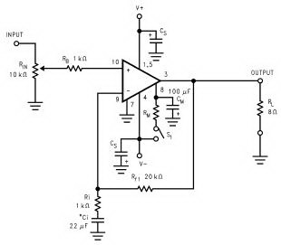
Download :
  • Parts Layout on Circuit Board
  • Diagram showing wiring of R61 and R63 to the sockets of Q18, Q20, Q28, and Q30 in the heat sink channel. 
  • Circuit Diagram 
  • Circuit Board Foil Pattern 
  • Part Layout with Underlying Traces
Read more

Wednesday, October 29, 2014

Temperature Candle Using LED

LED based projects require a lot of skill and hence only experienced circuit designers try out these circuits. But there are also a few circuits in this genre that can be done by amateur electronic hobbyists. The temperature candle is one such circuit. Read on to know more about this.

Temperature

The hardware components that are required to build this circuit are listed below:
- Microcontroller
- Temperature Sensor
- RGB LED
- PCB

The circuit design is pretty simple. The LED is made to flicker by the microcontroller and the color is based on the ambient temperature at that point. The temperature of the room can be known by observing the color of the LED.

The temperature value is obtained in degree Celsius. This value is received as a result of pressing the reset button on the PCB. This value can also be obtained by providing power to the device. Once the device is powered up, the change in temperature is indicated. The blue LED is triggered for a temperature increase of 10 degrees. The red LED is triggered for a temperature increase of a single degree.

Suppose, the ambient temperature is 23 degrees celsius, The circuit works in such a way that the blue LED is made to blink twice and the red LED is made to blink 3 times. Soon after this, an orange colored flicker is observed as the LED goes into canfle mode.

Since through hole components are used in this circuit, it is very cheap to construct and the components can be easily soldered. The circuit also contains a jack for connecting to a Microchip Pickit 3 programmer / debugger. This reduces the complexity involved in code modification and download.
Read more

6V to 12V Converter Circuit with BD679 BC547

This is a design circuit for converter circuit. This circuit is based on transistor as controller the circuit. There are two types of transistor that is BC547 and BD679. This circuit is a simple design of converter or inverter. This is the figure of the circuit.

This inverter circuit can to 800mA of 12V power supply with a 6V. For example could you 12V Car Accessories (UK turning into a 6V?) Car. The circuit is simple, more than 75% efficiency and very helpful. By changing a few components you, you also change for different voltages.

Electronic Part List

R1, R4 2 .2 K 1/4W Resistor

R2, R3 47K 1/4W Resistor

R5 1K 1/4W Resistor

R6 15K 1/4W Resistor

R7 33K 1/4W Resistor

R8 10K 1/4W Resistor

C1, C2 0.1uF Ceramic Disc Capacitor

C3 470uF 25V electrolytic capacitor

1N914 diode D1

D2 Diode 1N4004

D3 12V 400mW Zener Diode

Q1, Q2, Q4 BC547 NPN transistor

BD679 NPN transistor Q3

L1 See Notes

Notes

1. L1 is a custom inductor wound with about 80 turns 0.5 mm magnet wire a ring around the core with an outer diameter of 40 mm.

2. Different values of D3 can be used to obtain different output voltages from 0.6V to 30V is about. Note that at higher voltages, the circuit could perform just as well and can not produce much electricity. You may need to use a larger C3 for higher voltages and / or higher currents.
3. You can use a larger value for C3, in order to achieve a better filtering.
4. The circuit requires about 2A from the 6V supply to provide the full 800mA at 12V.
Read more

Tuesday, October 28, 2014

Two Colour LED Lights Bar

This circuit is a circuit run on alternating two insignia.It uses the 2-color LED with a built-participating in 3-pin single.This preference look for away the glow of every LED until the base.It turns alternating to one more color.In in the least way to the moon on the moon essential end, afterward the LED end of the first LED.Circuit consists of, nand gate ic.Two 10 Counter circuits IC, and IC JK flip washout .Company of the circuit is not speaking into 3 sets.It is a solid of gesture generators, a set of parade and control.Set the signal generator is IC1a,and IC1b quantity 4011 is a signal generator.The R2, R3, C2 determine the frequency generated.The hint is fed to a set of impressions is the figure 4011 IC2 and IC3.The 10 counter circuits to output to the LED, and Is the same, but the effort should ensue performed individual by the side of region.

Two

Therefore, the show from pin 11 of IC 2 and tested pro D2 and D3,To pin 3 of IC4.The integrated circuit IC 4 is a JK flip slump is connected to a T flip flop.The signal input pin 3 and pin 1 is the output hint at.Which sends a signal to the Reset IC either obstruct working.IC4 on the anniversary, it want output the originally moment in time, happening contrast to pin1.IC3 progress to handiwork, IC2 stopped.
IC2 is controlled by signals from pin 1 of IC4, to IC1c.earlier to control IC2.The IC3 is connected to pins 1 through D1 to the control again
Read more