Showing posts with label using. Show all posts

Friday, November 14, 2014

Digital to Analog Converter using Binary Weighted Resistors R 2R

The R-2R ladder DAC which is a binary-weighted DAC that uses a repeating cascaded structure of resistor values R and 2R. This improves the precision due to the relative ease of producing equal valued-matched resistors (or current sources). However, wide converters perform slowly due to increasingly large RC-constants for each added R-2R link. The D/A converter using binary-weighted resistors is shown in the figure below. In the circuit, the op-amp is connected in the inverting mode. The op-amp can also be connected in the non-inverting mode. The circuit diagram represents a 4-digit converter. Thus, the number of binary inputs is four.

Circuit Diagram


Fig. 1
We know that, a 4-bit converter will have 24 = 16 combinations of output. Thus, a corresponding 16 outputs of analog will also be present for the binary inputs.

Four switches from b0 to b3 are available to simulate the binary inputs: in practice, a 4-bit binary counter such as a 7493 can also be used.

Working

The circuit is basically working as a current to voltage converter.

1. b0 is closed
It will be connected directly  to the +5V.
Thus, voltage across R = 5V
Current through R = 5V/10kohm = 0.5mA
Current through feedback resistor, Rf = 0.5mA (Since, Input bias current, IB is negligible)
Thus, output voltage = -(1kohm)*(0.5mA) = -0.5V

2. b1 is closed, b0 is open
R/2 will be connected to the positive supply of the +5V.
Current through R will become twice the value of current (1mA) to flow through Rf.
Thus, output voltage also doubles.

3. b0 and b1 are closed
Current through Rf = 1.5mA
Output voltage = -(1kohm)*(1.5mA) = -1.5V

Thus, according to the position (ON/OFF) of the switches (bo-b3), the corresponding “binary-weighted” currents will be obtained in the input resistor. The current through Rf will be the sum of these currents. This overall current is then converted to its proportional output voltage. Naturally, the output will be maximum if the switches (b0-b3) are closed,

V0 = -Rf *([b0/R][b1/(R/2)][b2/(R/4)][b3/(R/8)]) 
Where each of the inputs b3, b2, b1, and b0 may either be HIGH (+5V) or LOW (0V).

The graph with the analog outputs versus possible combinations of inputs is shown below.

Fig. 2
The output is a negative going staircase waveform with 15 steps of -).5V each. In practice, due to the variations in the logic HIGH voltage levels, all the steps will not have the same size. The value of the feedback resistor Rf changes the size of the steps. Thus, a desired size for a step can be obtained by connecting the appropriate feedback resistor. The only condition to look out for is that the maximum output voltage should not exceed the saturation levels of the op-amp. Metal-film resistors are more preferred for obtaining accurate outputs.

Disadvantages

If the number of inputs (>4) or combinations (>16) is more, the binary-weighted resistors may not be readily available. This is why; R and 2R method is more preferred as it requires only two sets of precision resistance values.

Read more

Friday, October 31, 2014

Heat Detector Alarm using UM3561 Circuit Diagram

A very simple heat detector alarm electronic project can be designed using the UM3561 sound generator circuit and some other common electronic parts . This heat detector electronic circuit project uses a complementary pair comprising npn and pnp transistor to detect heat Collector of T1 transistor is connected to the base of the T2 transistor , while the collector of T2 transistor is connected to RL1 relay T3 and T4 transistors connected in darlington configuration are used to amplify the audio signal from the UM3561 ic.

Circuit
When the temperature close to the T1 transistor is hot , the resistance to the emitter –collector goes low and it starts conducting . In same time T2 transistor conducts , because its base is connected to the collector of T1 transistor and the RL1 relay energized and switches on the siren which produce a fire engine alarm sound. This electronic circuit project must be powered from a 6 volts DC power supply , but the UM3561 IC is powered using a 3 volt zener diode , because the alarm sound require a 3 volts dc power supply. The relay used in this project must be a 6 volt / 100 ohms relay and the speaker must have a 8 ohms load and 1 watt power.
Read more

Headphone Amplifier Using Discrete Components

An amplifier to drive low to medium impedance headphones built using discrete components.

Both halves of the circuit are identical. Both inputs have a dc path to ground via the input 47k control which should be a dual log type potentiometer. The balance control is a single 47k linear potentiometer, which at center adjustment prevents even attenuation to both left and right input signals. If the balance control is moved towards the left side, the left input track has less resistance than the right track and the left channel is reduced more than the right side and vice versa. The preceding 10k resitors ensure that neither input can be "shorted" to earth.

Circuit diagram:Headphone
Headphone Amplifier Circuit Diagram

Amplification of the audio signal is provided by a single stage common emitter amplifier and then via a direct coupled emitter follower. Overall gain is less than 10 but the final emitter follower stage will directly drive 8 ohm headphones. Higher impedance headphones will work equally well. Note the final 2k2 resistor at each output. This removes the dc potential from the 2200u coupling capacitors and prevents any "thump" being heard when headphones are plugged in. The circuit is self biasing and designed to work with any power supply from 6 to 20 Volts DC
Read more

Wednesday, October 29, 2014

Temperature Candle Using LED

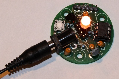
LED based projects require a lot of skill and hence only experienced circuit designers try out these circuits. But there are also a few circuits in this genre that can be done by amateur electronic hobbyists. The temperature candle is one such circuit. Read on to know more about this.

Temperature

The hardware components that are required to build this circuit are listed below:
- Microcontroller
- Temperature Sensor
- RGB LED
- PCB

The circuit design is pretty simple. The LED is made to flicker by the microcontroller and the color is based on the ambient temperature at that point. The temperature of the room can be known by observing the color of the LED.

The temperature value is obtained in degree Celsius. This value is received as a result of pressing the reset button on the PCB. This value can also be obtained by providing power to the device. Once the device is powered up, the change in temperature is indicated. The blue LED is triggered for a temperature increase of 10 degrees. The red LED is triggered for a temperature increase of a single degree.

Suppose, the ambient temperature is 23 degrees celsius, The circuit works in such a way that the blue LED is made to blink twice and the red LED is made to blink 3 times. Soon after this, an orange colored flicker is observed as the LED goes into canfle mode.

Since through hole components are used in this circuit, it is very cheap to construct and the components can be easily soldered. The circuit also contains a jack for connecting to a Microchip Pickit 3 programmer / debugger. This reduces the complexity involved in code modification and download.
Read more

Saturday, October 18, 2014

PIC18F2620 Etching pan rocker

Some people consider PCB etching as a tedious task. One has to have extra care in handling the etchant – which stains, one needs to keep an eye on it to avoid over etching and one needs to rock the etching pan to speed up the etching process.
To make life a lot easier for hobbyists Graham came up with an ingeniously simple way of automating the rocking motion for the etching pan. He attached a servo motor on a pivot where the etching pan can tilt on both directions. Using a PIC18F2620 to send digital pulses he controls the back and forth motion of the servo which in turn gives the etching pan a rocking motion. Rock A By etching pan.
Read more

Breadboard module using A PIC16F628A

You don’t usually see microcontroller projects in a breadboard and I’ll give you one reason why – microcontrollers require some external components that eventually consumes the prototyping space in a breadboard. This is one of the reasons why hobbyists prefers to make/test projects in a custom PCB rather than the good old breadboard.
To remedy the dilemma of prototyping a PCB just to test a microcontroller circuit, R-B had this very fancy idea of making a breadboard module for a microcontroller. The module’s main part is a PIC16F628A, all the external components to make the microcontroller functional is also placed in the board – oscillator crystal, pull up resistor for the MCLR and even the reset button are already in the board. The only pins that sticks out of the module are the I/O pins and the power pins. Now people can verify microcontroller circuits without fabricating a specific board.
Read more

Thursday, October 2, 2014

Adjustable Voltage Current Power Supply Circuit Using IC L200

  1.  IC2 is connected as a differential amplifier and compares the signals at its two inputs.
  2. Referring to the circuit diagram: the input comprises a mains switch, fuse, transformer, bridge rectifier and smoothing capacitor (C2).
  3. The difference between the inputs is the voltage drop across current’ sensor R4. This IC feeds the current sensing input (pin 2) of the L200.
  4. P1 in the feedback loop of the 741 is used to vary the output current of the circuit. IC1 must be mounted on a suitable heat sink as it dissipates nearly all the power of the circuit.
  5. The reference level output from I pin 4 of IC1 goes to the voltage divider made up of R5 and P2 (this pot sets the value of the output voltage).
  6. The power supply can quite easily be built into a case and a voltmeter and ammeter mounted on the front panel. ln view of the accuracy of the circuit these should ideally be digital meters, but virtually any type will do.
  7. If you compare the expense and the rating of this power supply you will get a surprise, because the output voltage and current are fully adjustable between O. . . 18 V and 0 . . . 1.8 A respectively and costs have still been kept very reasonable.
  8. Diode D5 and capacitor C1 produce a negative auxiliary voltage, which is stabilized by zener diode D6 and capacitor C4.
  9. All this is necessary to enable the output voltage to be adjusted down to zero volts. During the construction of this part of the circuit bear in mind that the positive lead of electrolytic capacitor C4 is connected to earth! Regulation is provided by IC1 and IC2. Capacitor C3 suppresses any residual transients at the input of lC1 and it should therefore be connected as closely as possible to IC1 similarly C4 and IC2).
  10. The negative voltage provides the negative supply for the two ICs. 

Read more

Friday, September 26, 2014

Active Tone Control Circuit Using a Single Opamp

The input signal is applied to the non-inverting input of the lC which is a Siemens TAA861 operational amplifier.
Bass and treble boost and cut are con_trolled by the potentiometers RV1 and RV2 respectively. Control range is 20 dB of boost or cut at 50 Hz and 15 dB boost or 20 dB of cut at 12 kHz. The overall gain of the circuit at 1 kHz is 15dB and the input impedance is greater than 80 k ohm. Total harmonic distortion for 2.4 volts output is less than 0.5% and remains below 4% for up to 3.5 volts output. Correct law for the potentiometer is antilog. This may be obtained by using slide potentiometers which are mounted in reverse (end-for~end) to normal. Note that equalization is not incorporated in this preamplifier.


This simple single-transistor circuit will give approximately 15 dB boost or cut at 100 Hz and 15 kHz respectively. A low noise audio type transistor is used, and the output can be fed directly into any existing amplifier volume control to which the tone control is to be fitted. A The gain of the circuit is near unity when controls are set in the "flat" position. 


Read more

Wednesday, September 24, 2014

Simple Solar charger circuit project using transistors

A very simple solar charger circuit project can be designed using few external electronic parts . This simple solar charger circuit is capable of handling charge currents of up to 1A. Alternate component values are given in the figure for lower current applications.

Circuit diagram:
12V-SLA-chargher Solar charger circuit project using transistors circuit diagram

The only adjustment is the voltage trip point when the current is shunted through the transistor and load resistor. This should be set with a fully charged battery. As the transistor and R3 have the entire panel’s output across them when the battery is fully charged, all of the current from the panel will be going through R3 and the Darlington transistor TIP112, so these must be well heat sunk. Adjust R1 for the trip point, usually 14.4 V – 15 V for a 12 V SLA or a 12 V Ni-Cd battery.


source : Link
Read more

Supply Variable 1V to 9V Circuit using Power PC

This is a variable power supply which converts an input voltage from 12V SMPS / PSU a desktop computer, to an output voltage from 1.25 to 9 volts. This converter will be very useful for electronics hobbyists. 

The circuit uses a LM317T regulator IC that can reach up to 1 ampere, the diode D1 protects against polarity reversal and the diode D2 keeps the output voltage from the input voltage increases when an inductive or capacitive load is connected to the output.Similarly, the capacitor C3 removes any residual noise of the line regulates the voltage potentiometer VR1.


Supply Variable 1V to 9V  using Power PC Circuit Diagram

Supply Variable 1V to 9V Circuit using Power PC

Read more

Temperature Candle Using LED

LED based projects require a lot of skill and hence only experienced circuit designers try out these circuits. But there are also a few circuits in this genre that can be done by amateur electronic hobbyists. The temperature candle is one such circuit. Read on to know more about this.

Hacks and Mods: Temperature Candle Using LED

The hardware components that are required to build this circuit are listed below:
  • Microcontroller
  • Temperature Sensor
  • RGB LED
  • PCB

The circuit design is pretty simple. The LED is made to flicker by the microcontroller and the color is based on the ambient temperature at that point. The temperature of the room can be known by observing the color of the LED.

The temperature value is obtained in degree Celsius. This value is received as a result of pressing the reset button on the PCB. This value can also be obtained by providing power to the device. Once the device is powered up, the change in temperature is indicated. The blue LED is triggered for a temperature increase of 10 degrees. The red LED is triggered for a temperature increase of a single degree.
Suppose, the ambient temperature is 23 degrees celsius, The circuit works in such a way that the blue LED is made to blink twice and the red LED is made to blink 3 times. Soon after this, an orange colored flicker is observed as the LED goes into canfle mode.

Since through hole components are used in this circuit, it is very cheap to construct and the components can be easily soldered. The circuit also contains a jack for connecting to a Microchip Pickit 3 programmer / debugger. This reduces the complexity involved in code modification and download.
Read more

Small Audio Amplifiers Using LM386 and NE5534

Many electronic projects require the use of a small audio amplifier. Be it a radio transceiver, a digital voice recorder, or an intercom, they all call for an audio amp that is small, cheap, and has enough power to provide adequate loudness to fill a room, without pretending to serve a disco! About one Watt RMS seems to be a convenient size, and this is also about the highest power that a simple amplifier fed from 12V can put into an 8 Ohm speaker. A very low saturation amplifier may go as high up as 2 Watt, but any higher power requires the use of a higher voltage power supply, lower speaker impedance, a bridge circuit, or a combination of those.

During my many years building electronic things I have needed small audio amps many times, and have pretty much standardized on a few IC solutions, first and and foremost the LM386, which is small, cheap, and very easy to use. But it does not produce high quality audio... For many applications, the advantages weigh more than the distortion and noise of this chip, so that I used it anyway. In other cases I used different chips, which perform better but need more complex circuits. Often these chips were no longer available the next time I needed a small amplifier.

When I last upgraded my computer, I replaced the old and trusty Soundblaster AWE 32 by a Soundblaster Audigy. The new card is better in many regards, but while the old one had an internal audio power amplifier, the new one doesnt! Thats bad news, because I have some pretty decent speakers for the PC, which are fully passive. So, I built a little stereo amp using two LM386 chips and installed it inside the computer, fed by the 12V available internally.

But then I wasnt satisfied. The LM386 might be suitable for "communication quality" audio, which is roughly the fidelity you get over a telephone, but for music its pretty poor! The distortion was awful. So, the day came when I decided to play a little more scientifically with small audio amps, looking for a way to get good performance with simple and inexpensive means.

I set up a test bench with a sine wave oscillator running at 1 kHz, an 8 Ohm speaker, 12V power supply, and the computer with the soundcard and Fast Fourier Transform software. One channel was connected to the oscillator together with the amplifier input, the other channel to the output and speaker. With this setup I measured the harmonic content of the audio signals. I did the tests at an output level of 0.1W, which is typical for moderately loud sound from a reasonably efficient speaker. Also, I used a music signal from a CD player to test the actual sound of each amplifier.

Circuit Project: Small Audio Amplifiers Using LM386 and NE5534

As already said above, the main attraction of the LM386 is the extreme simplicity of its application circuit. You can even eliminate R1 if the signal source is DC-grounded. If the speaker leads are long, you should add an RC snubber across the output to aid stability. Additionally, if you need higher gain (not necessary if the input is at line level), you can connect a 10uF capacitor between pins 1 and 8. Thats about all there is to it.

Now the bad news: This circuit produced a very high level of distortion! The second harmonic measured just -28dB from the main output. The third harmonic was at -35dB, while the noise level was at -82dB. There were assorted high harmonics at roughly -45dB. With music, the distortion was really disturbing, and also the noise level was uncomfortably high. The power supply rejection is poor, so that some hum and other supply noise gets through. In short, this was a lousy performance!

Since I had used so many LM386s in my projects, I had several different variations. In my material box I found a slightly newer LM386N-1. So I plugged it into my test amplifier. It was even worse! The second harmonic was at -24dB, the third harmonic at -31dB, while the noise was a tad better at -84dB. Folks, thats a total harmonic distortion of almost 7%! And the 0.1W output level at which this was measured is where such a circuit is about at its best...  The distortion can be plainly seen on the oscilloscope, and a visibly distorted waveform is about the most offending thing an audio designer can ever see!

Looking through my projects, I found one where I had used a GL386 chip. This is just a 386 made by another company. I unsoldered it and put it in my test amplifier. Surprise! It was dramatically better, with the second harmonic at -45dB, and the third at -57dB! The noise floor was -84dB, just like the LM386N-1. But even this level of distortion was plainly audible when listening to music. Thats roughly 0.6% THD. Some folks may consider it acceptable for music. I dont, but for communication equipment its fine. At this point, I decided to see if I could build a better amplifier, that doesnt become too complex nor expensive.

Circuit Project: Small Audio Amplifiers Using LM386 and NE5534

This was the first attempt. A low distortion, fast slew rate, but easy to find and rather inexpensive operational amplifier, driving a simple source follower made of two small transistors. These transistors are not biased, so they work at zero quiescent current, in full class B. The only mechanism that works against crossover distortion here is the high slew rate of the OpAmp, which is able to make the distortion bursts during crossover very short. To say the truth, I didnt expect to get usable performance from this circuit, and was really surprised when it worked much better than the 386! The second harmonic was at -77dB, the third at -79dB!

Also there were many high harmonics at roughly -84dB. That means a THD of about 0.015%.  The noise floor was down at the -120dB level! The power supply rejection was excellent, with no detectable feedtrough. Playing music, this amplifier sounded really good: No audible noise, and the distortion could be heard when paying attention to it, but I doubt that the average person would detect it! Not bad, for a bias-less design!

Just to see how important the slew rate of the OpAmp is, I pulled out the NE5534 and replaced it by a humble 741, which is many times slower. The result was dramatic: The second harmonic still good at -70dB, but the third harmonic was much worse, at -48dB. Also there were many high harmonics at the same -48dB level. Given that second harmonic distortion doesnt sound bad to most people, but third harmonic does, and high harmonics are even worse, it came as no surprise that the amplifier with the 741 sounded bad.

At low volume it sounded particularly bad! So I returned to the oscillator and measurement setup, testing at lower output power, and found that while the second and third harmonics followed the output, the high harmonics stayed mostly constant! So, at very low output, the high harmonics became very strong relative to the output. All this is the effect of the slower slew rate of the 741, which makes it less effective correcting the crossover distortion of the unbiased transistors. Interestingly, the noise floor of the 741 circuit wasnt bad: -118dB.

Just for fun, I tried this circuit with a third OpAmp: The TL071, which is good, but not as good as the 5534. The results: Second harmonic at -72dB, third and the high ones at -60dB, and the noise at -120dB. Its interesting that the second harmonic is much more suppressed than the third one. That must be a balancing effect of the symmetric output stage, and the better symmetry in the TL071 compared to other OpAmps.

Its worthwhile to note that this amplifier can be simplified a lot by using a split power supply. R1, R2, C1, C2 and C4 would be eliminated! But then you need the capacitor removed from C4 to bypass the negative supply line. The positive input of the chip goes to ground, while pin 4 and the collector of Q2 go to the negative supply. The rest stays the same. If you use a +-15V supply, the available RMS output power grows to over 10 Watt! Of course, you then need larger transistors. And since larger transistors are slower, the distortion will rise somewhat. An added benefit of a split supply is that the popping noise when switching on and off is eliminated.

Circuit Project: Small Audio Amplifiers Using LM386 and NE5534

As the next experiment, I decided to get rid of the crossover distortion. For this purpose, I added a traditional adjustable bias circuit with a transistor and a trimpot. Now I also had to add a current source, because with the bias circuit there is no single point into which the OpAmp could put its drive current into both bases! I adjusted the bias for the best distortion, and this was really  a good one! The second harmonic was down right where the test oscillator delivered it, about -80dB, so I couldnt really measure it!

The third harmonic was at -84dB, and the best improvement was that the higher harmonics had simply disappeared! They were all below the noise floor, which stayed at -120dB. Actually, this noise floor seems to come from the soundcard A/D converter, so that the actual noise of this and the above amplifier may even be better! With music, this amplifier sounded perfect - clean and smooth. And Im pretty confident that the THD is well below the limits of my measurement setup, which is 0.01%.

The quiescent current was around 10mA. When lowering it to about 3mA, the high harmonics started to rise out of the noise floor. If you want to adjust the bias for the exact best quiescent current, there is a simple trick: Lift R4 from the output, and connect it to pin 6. Now the output stage has been left outside the feedback loop, and all its distortion will show up at the output. Watching the signal on an oscilloscope, or even better on a real time spectrum analyzer (soundcard and software), adjust the trimpot to the lowest distortion level.

Have a current meter in the supply line and make sure that you dont exceed 30mA or so of quiescent current, in order to keep the small transistors cool. But most likely the best distortion will be at a current lower than that. Once the adjustment is complete, return R4 to its normal position. Now the full gain and slew rate of the operational amplifier is used to correct the small remaining cross-over distortion of the output stage, and the distortion will certainly disappear from the scope screen, from your ears, and possibly fall below the detection level of the spectrum analyzer!

This circuit can also be run from a split power supply, by exactly the same mods as for the previous circuit. And since the transistors are properly biased, there isnt any significant distortion increase when using larger transistors. Be sure to use some that have enough gain - you have only a few mA of driving available, and with a +-15V power supply and an 8 Ohm speaker, there can be almost 2A of output current! So, you need a gain of 300 at least. There are power transistors in the 4A class that provide such gain, and these are good candidates. The other option is using Darlington transistors, which far exceed the gain needed here. But they will again increase the distortion, not very much, but perhaps enough to make it audible again.
 
 
Source: Humo Luden
Read more

Friday, September 19, 2014

Simple Power Pulse Using by LM350 and NE555 Circuit Diagram

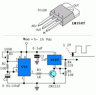
This Power Pulse Using by LM350 and NE555 Circuit Diagram can use to drive lamp,power LED,DC motor etc. Adjust R5 for output amplitude.Adjust R1 for output power .The LM350 is adjustable 3-terminal positive voltage regulators is capable of supplying in excess of 3A over a 1.2V to 33V output range.This circuit requires 5-15V power supply.


Power Pulse Using by LM350 and NE555 Circuit Diagram

Power Pulse Using by LM350 and NE555 Circuit Diagram


Read more